www.ti.com
PCB Layout Guideline
2.4.4 Charger Cut-Off by Thermistor
1. Slowly increase the output voltage of PS2 until Ibat = 0 ± 10mA.
Measure → V(J4(TS)) = 2.44V ± 200mV
Observe → D7 (STAT1) off; D8 (STAT2) off.
2. Slowly decrease the output voltage of PS2 to 1.4V ± 0.1V.
Measure → V(J4(TS)) = 1.4V ± 100mV
Measure → Ibat = 3000mA ± 300mA (bq24610/617)
Measure → Ibat = 0mA ± 100mA (bq24616)
Measure → Ibat = 375mA ± 150mA (bq2463x)
Observe → D7 (STAT1) on; D8 (STAT2) off (bq24610/617/630)
Observe → D7 (STAT1) off; D8 (STAT2) off (bq24616)
3. Slowly decrease the output voltage of PS2.
Charge will resume. Continue to decrease the output voltage of PS2 slowly until Ibat = 0 ±10mA.
Measure → V(J4(TS)) = 1.14V ± 200mV
Observe → D7 (STAT1) off; D8 (STAT2) off.
4. Slowly increase the output voltage of PS2 to 1.8V ± 100mV.
Measure → Ibat = 3000mA ± 200mA
Observe → D7 (STAT1) on; D8 (STAT2) off.
2.4.5 Power Path Selection
1. Take off JP5 (Disable the charging)
Observe → D3 (CE) off; D7 (STAT1) off.
2. Set JP3 Jumper On 2-3 (VPULLUP and VEXT). Connect the output of the power supply #3 to
J2(VEXT, GND). Set the power supply #3 for 3.3V ± 200mVDC, 1.0 ± 0.1A current limit.
3. Set the Load #2 output voltage to 16.5V ± 500mV.
4. Measure → V(J5(SYS)) = 24V ± 1V (adapter connected to system)
Observe → D4 (ACDRV) on, D6 (BATDRV) off, D5 (PG) on, D7 (STAT1) off, D8 (STAT2) off.
5. Turn off PS#1.
6. Measure → V(J5(SYS)) = 16.5V ± 0.5V (battery connected to system)
7. Observe → D4 (ACDRV) off, D6 (BATDRV) on, D5 (PG) off, D7 (STAT1) off, D8 (STAT2) off.
8. Turn off power supply #2 and #3. Set JP3 on 1-2 (VPULLUP and VREF).
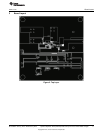
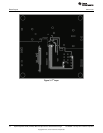
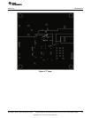
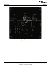
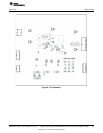
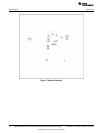
3 PCB Layout Guideline
1. It is critical that the exposed power pad on the backside of the bq2461x/bq2463x package be soldered
to the PCB ground. Make sure there are sufficient thermal vias right underneath the IC, connecting to
the ground plane on the other layers.
2. The control stage and the power stage should be routed separately. At each layer, the signal ground
and the power ground are connected only at the power pad.
3. AC current sense resistor must be connected to ACP and ACN with a Kelvin contact. The area of this
loop must be minimized. The decoupling capacitors for these pins should be placed as close to the IC
as possible.
4. Charge current sense resistor must be connected to SRP, SRN with a Kelvin contact. The area of this
loop must be minimized. The decoupling capacitors for these pins should be placed as close to the IC
as possible.
5. Decoupling capacitors for DCIN, VREF, VCC, REGN should make the interconnections to the IC as
short as possible.
6. Decoupling capacitors for BAT must be placed close to the corresponding IC pins and make the
interconnections to the IC as short as possible.
7. Decoupling capacitor(s) for the charger input must be placed close to top buck FET's drain and bottom
buck FET’s source.
7
SLUU396A–January 2010–Revised July 2010 bq2461x/bq2463x EVM (HPA422) Multi-Cell Synchronous Switch-Mode Charger
Copyright © 2010, Texas Instruments Incorporated


