2002 May 22 14
Philips Semiconductors Product specification
Low power audio DAC UDA1334BT
14.3 Timing
V
DDD
=V
DDA
= 1.8 to 3.6 V; T
amb
= −20 to +85 °C; R
L
=5kΩ; all voltages with respect to ground (pins V
SSA
and V
SSD
);
unless otherwise specified; note 1.
Note
1. The typical value of the timing is specified at f
s
= 44.1 kHz (sampling frequency).
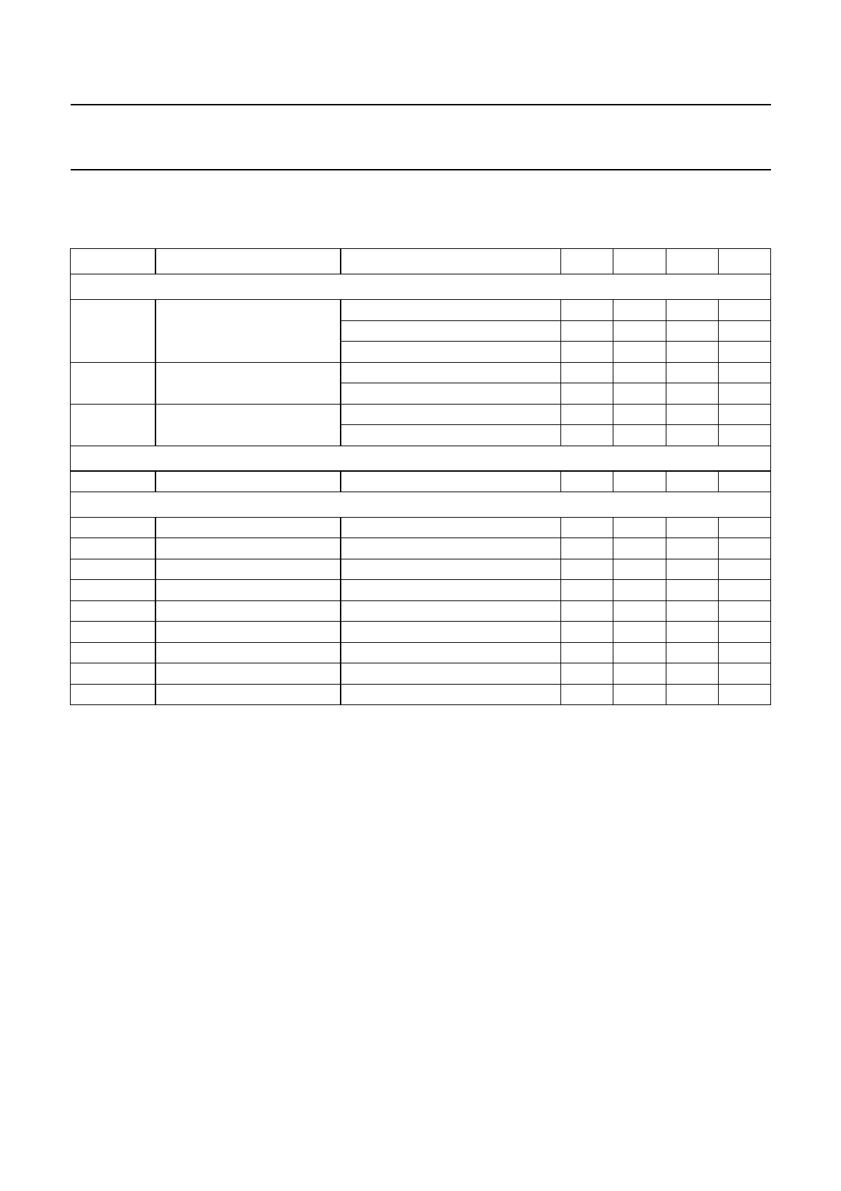
SYMBOL PARAMETER CONDITIONS MIN. TYP. MAX. UNIT
System clock timing (see Fig.6)
T
sys
system clock cycle time f
sys
= 256f
s
35 88 780 ns
f
sys
= 384f
s
23 59 520 ns
f
sys
= 512f
s
17 44 390 ns
t
CWH
system clock HIGH time f
sys
< 19.2 MHz 0.3T
sys
− 0.7T
sys
ns
f
sys
≥ 19.2 MHz 0.4T
sys
− 0.6T
sys
ns
t
CWL
system clock LOW time f
sys
< 19.2 MHz 0.3T
sys
− 0.7T
sys
ns
f
sys
≥ 19.2 MHz 0.4T
sys
− 0.6T
sys
ns
Reset timing
t
reset
reset time 1 −−µs
Serial interface timing (see Fig.7)
f
BCK
bit clock frequency −−64f
s
Hz
t
BCKH
bit clock HIGH time 50 −−ns
t
BCKL
bit clock LOW time 50 −−ns
t
r
rise time −−20 ns
t
f
fall time −−20 ns
t
su(DATAI)
set-up time data input 20 −−ns
t
h(DATAI)
hold time data input 0 −−ns
t
su(WS)
set-up time word select 20 −−ns
t
h(WS)
hold time word select 10 −−ns


