


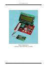


SK-TSC-1125S User Guide
- 12 - © Fujitsu Microelectronics Europe GmbH
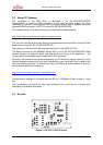
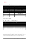
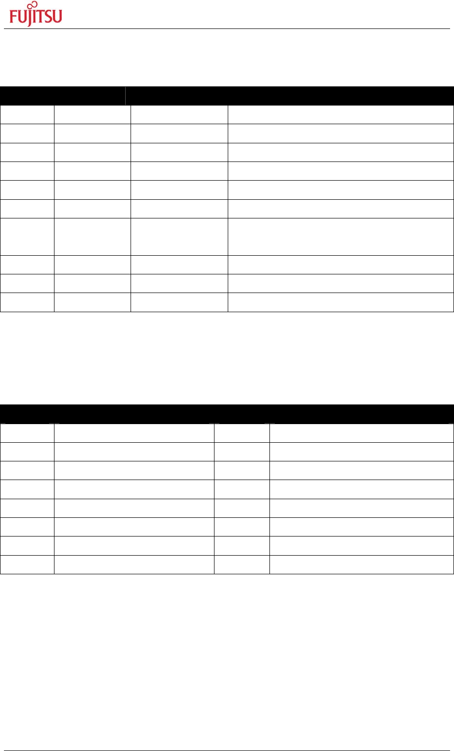
2.5 I2C header (X1) pinout (ADA-16FX-TSC-LCD)
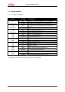
X5 Pin Name Connected to Descripton
1 SCL JP6, X3 Pin 1 I2C Serial Clock Line
2 SDA JP4, X3 Pin 2 I2C Serial Data Line
3 GND System Ground
4 VCC VCC for TSC and LCD
5 TINT X3 Pin 5 Touch interrupt from TSC to MCU
6 GINT X3 Pin 6 General Purpose interrupt from TSC to MCU
7 TOUT X3 Pin 7
‘Beep’ Signal for Piezo Buzzer
(FMA1127-40N only)
8 RESET_N X3 Pin 8 Reset Pin of TSC
9 reserved X4 Pin 1
10 reserved X4 Pin 2
X3 can be used to access the TSC signals, e.g. to route the Interrupts to an appropriate
external interrupt pin of the MCU.
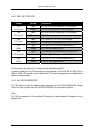
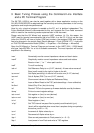
2.6 LCD header (X5) pinout (ADA-16FX-TSC-LCD)
Pin Name Pin Name
1 VSS 9 n/c
2 VDD 10 n/c
3 V0 (contrast) 11 D4
4 RS 12 D5
5 R/W 13 D6
6 E 14 D7
7 n/c 15 VLED (Backlight +)
8 n/c 16 VLSS (Backlight -)
The contrast for the (optional) LC display can be adjusted using RP1.
2.7 Further connection options
Using X3 (VCC), X4 (GND) and X2 (GPIO0 – 3), additional connections to the FMA1125 can
be made. X2 is connected to the digital input / output pins GPIO0-3 of the TSC. If these are
to be connected to external circuits, the on-board LEDs can be disabled by opening JP3.