


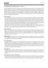
– 3 –
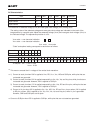
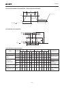
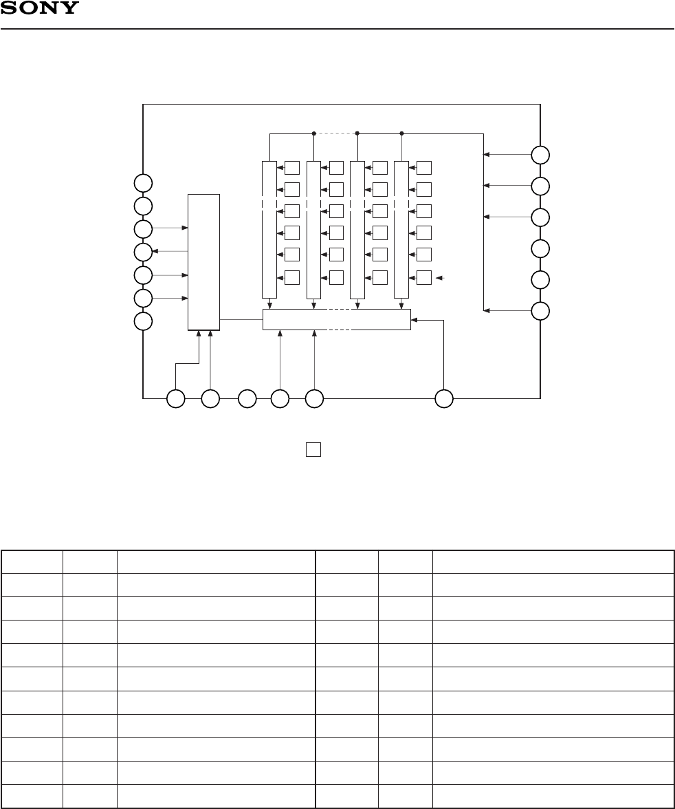
ICX423AL
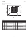
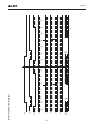
Block Diagram and Pin Configuration
(Top view)
Horizontal Register
Output Unit
Note)
Note) : Photo sensor
GND
V
DD
SUB
RG Hφ
1
Vertical Register
HIS
V
OUT
Vφ
4
Vφ
3
Vφ
2
Vφ
1
V
L
GND
V
GG
V
SS
GND
RD Hφ
2
V
L
7
9
10
11
12
13
14
15 16 17 18 19 20
6
5
4
3
2
1
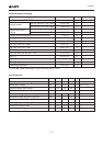
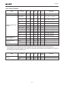
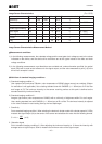
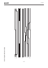
Pin Description
Pin No. Symbol Description
1
2
3
4
5
6
7
8
9
10
Vφ4
Vφ3
Vφ2
SUB
GND
Vφ1
VL
NC
GND
VDD
Signal output
Output amplifier gate bias
Output amplifier source
GND
Reset drain
Reset gate clock
Protective transistor bias
Horizontal register transfer clock
Horizontal register transfer clock
Horizontal register input source bias
Description
Pin No. Symbol
Vertical register transfer clock
Vertical register transfer clock
Vertical register transfer clock
Substrate (overflow drain)
GND
Vertical register transfer clock
Protective transistor bias
GND
Output amplifier drain power
11
12
13
14
15
16
17
18
19
20
VOUT
VGG
VSS
GND
RD
RG
VL
Hφ1
Hφ2
HIS