


– 4 –
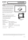
ICX423AL
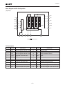
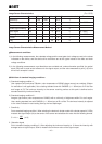
Absolute Maximum Ratings
Item
HIS, VDD, RD, VOUT, VSS – GND
HIS, VDD, RD, VOUT, VSS – SUB
Vertical clock input pins – GND
Vertical clock input pins – SUB
Substrate voltage SUB – GND
Supply voltage
Vertical clock input
voltage
Voltage difference between vertical clock input pins
Voltage difference between horizontal clock input pins
Hφ1, Hφ2 – Vφ4
Hφ1, Hφ2, RG, VGG – GND
Hφ1, Hφ2, RG, VGG – SUB
VL – SUB
Vφ1, Vφ3, HIS, VDD, RD, VOUT – VL
RG – VL
Vφ2, Vφ4, VGG, VSS, Hφ1, Hφ2 – VL
Storage temperature
Operating temperature
–0.3 to +55
–0.3 to +20
–55 to +10
–15 to +20
to +10
to +15
to +17
–17 to +17
–10 to +15
–55 to +10
–65 to +0.3
–0.3 to +30
–0.3 to +24
–0.3 to +20
–30 to +80
–10 to +60
V
V
V
V
V
V
V
V
V
V
V
V
V
V
°C
°C
∗
1
Ratings
Unit Remarks
∗
1
27V (Max.) when clock width < 10µs, clock duty factor < 0.1%.
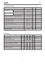
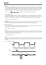
Output amplifier drain voltage
Reset drain voltage
Output amplifier gate voltage
Output amplifier source
Substrate voltage adjustment range
Substrate voltage adjustment precision
Reset gate clock voltage adjustment range
Reset gate clock voltage adjustment precision
Protective transistor bias
Horizontal register input source bias
Item
VDD
VRD
VGG
VSS
VSUB
∆VSUB
VRGL
∆VRGL
VL
VHIS
Symbol
14.7
14.7
3.8
9
–3
0
–3
–11
14.7
Min.
V
V
V
V
%
V
%
V
V
Unit
VRD = VDD
±5%
∗
2
∗
2
∗
3
VHIS = VDD
RemarksTyp. Max.
15.0
15.0
4.2
–10.5
15.0
15.3
15.3
4.6
19
+3
3.0
+3
–10
15.3
Bias Conditions
Ground with 750Ω resistor