PCB Layout Guideline
www.ti.com
5.2 Options for External Transistor
Using a Transistor in a TO-220 package
The EVM is populated with a DPAK transistor for Q1. However, if desired, a TO-220 transistor can be
used instead. Three holes have been placed in the PCB in parallel with the DPAK pad. Remove the DPAK
transistor and replace it with a TO-220 transistor. The top hole is the base, the middle hole is the collector,
and the bottom hole is the emitter.
Using a P-channel FET
The EVM is populated with a PNP transistor for Q1. However, if desired, a P-channel MOSFET may be
used instead. In order to use a P-FET, a resistor must be populated on R5. Pin 16 of the BQ24450 will
sink current through R5 and generate a negative gate to source voltage for the P-FET. By varying the sink
current (and subsequently Vgs), the IC can accurately control the charge current. A 1kΩ resistor is
suitable for R5.
Changing the topology
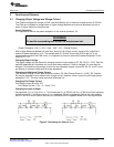
The EVM is configured with the Common-Emitter PNP topology. However, it can also be configured for
the PNP in a Quasi-Darlington as described on page 13 of the datasheet. To make this change, the
following steps should be taken:
1. Place jumper on JP3 such that it connects Pin 15 of the IC to the collector of Q1.
2. Remove R6 and replace with Rp as calculated on page 13 of the data sheet.
5.3 Other Options
Disabling Pre-Charge Mode
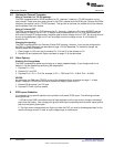
The EVM is populated to perform pre-charge on a deeply depleted battery. If pre-charge mode is not
desired, it can be disabled by performing the steps below.
1. Populate R1 = 0 Ω
2. Remove R11 and R12
3. Populate R14 = R11 + R12 (For example: If R11 = 75kΩ and R12 = 16.9kΩ, R14 = 91.9kΩ)
PGOOD
As populated, the EVM uses PGOOD as part of the feedback divider (explained on page 11 of data
sheet). If desired, PGOOD can be used to indicate the supply status on pin 5.
1. Remove R8 and place it on R15 pad.
2. Populate R13 with a pull-up resistor.
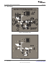
6 PCB Layout Guideline
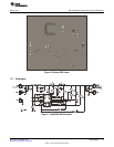
It is important to pay special attention to the printed-circuit board (PCB) layout. The following provides
some guidelines:
1. All low-current GND connections must be kept separate from the high-current charge or discharge
paths from the battery. Use a single-point ground technique incorporating both the small signal ground
path and the power ground path.
2. The high current charge paths into IN pin and from the OUT pin must be sized appropriately for the
maximum charge current in order to avoid voltage drops in these traces.
6
bq24450EVM SLUU464–November 2010
Submit Documentation Feedback
© 2010, Texas Instruments Incorporated


