


Ratiometric Linear Hall Effect Sensor
for High-Temperature Operation
A1321, A1322,
and A1323
3
Allegro MicroSystems, Inc.
115 Northeast Cutoff
Worcester, Massachusetts 01615-0036 U.S.A.
1.508.853.5000; www.allegromicro.com
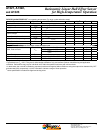
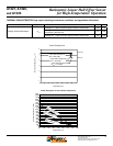
DEVICE CHARACTERISTICS
1
over operating temperature (T
A
) range, unless otherwise noted
Characteristic Symbol Test Conditions Min. Typ.
2
Max. Units
Electrical Characteristics; V
CC
= 5 V, unless otherwise noted
Supply Voltage V
cc(op)
Operating; Tj < 165°C 4.5 5.0 5.5 V
Supply Current I
cc
B = 0, I
out
= 0 – 5.6 8 mA
Quiescent Voltage V
out(q)
B = 0, T
A
= 25ºC, I
out
= 1 mA 2.425 2.5 2.575 V
Output Voltage
3
V
out(H)
B = +X, I
out
= –1 mA – 4.7 – V
V
out(L)
B = –X, I
out
= 1 mA – 0.2 – V
Output Source Current Limit
3
I
out(LM)
B = –X, V
out
→ 0 –1.0 –1.5 – mA
Supply Zener Clamp Voltage V
Z
I
cc
= 11 mA = I
cc(max)
+ 3 6 8.3 – V
Output Bandwidth BW – 30 – kHz
Clock Frequency f
C
– 150 – kHz
Output Characteristics; over V
CC
range, unless otherwise noted
Noise, Peak-to-Peak
4
V
N
A1321; C
bypass
= 0.1 μF, no load – – 40 mV
A1322; C
bypass
= 0.1 μF, no load – – 25 mV
A1323; C
bypass
= 0.1 μF, no load – – 20 mV
Output Resistance R
out
I
out
≤ ±1 mA – 1.5 3 Ω
Output Load Resistance R
L
I
out
≤ ±1 mA, VOUT to GND 4.7 – – kΩ
Output Load Capacitance C
L
VOUT to GND – – 10 nF
1
Negative current is defi ned as conventional current coming out of (sourced from) the specifi ed device terminal.
2
Typical data is at T
A
= 25°C. They are for initial design estimations only, and assume optimum manufacturing and application
conditions. Performance may vary for individual units, within the specifi ed maximum and minimum limits.
3
In these tests, the vector X is intended to represent positive and negative fi elds suffi cient to swing the output driver between fully OFF
and saturated (ON), respectively. It is NOT intended to indicate a range of linear operation.
4
Noise specifi cation includes both digital and analog noise.