


Ratiometric Linear Hall Effect Sensor
for High-Temperature Operation
A1321, A1322,
and A1323
9
Allegro MicroSystems, Inc.
115 Northeast Cutoff
Worcester, Massachusetts 01615-0036 U.S.A.
1.508.853.5000; www.allegromicro.com
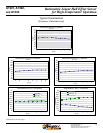
Power Derating
The device must be operated below the maximum junction
temperature of the device, T
J(max)
. Under certain combinations of
peak conditions, reliable operation may require derating sup-
plied power or improving the heat dissipation properties of the
application. This section presents a procedure for correlating
factors affecting operating T
J
. (Thermal data is also available on
the Allegro MicroSystems Web site.)
The Package Thermal Resistance, R
θJA
, is a fi gure of merit sum-
marizing the ability of the application and the device to dissipate
heat from the junction (die), through all paths to the ambient air.
Its primary component is the Effective Thermal Conductivity,
K, of the printed circuit board, including adjacent devices and
traces. Radiation from the die through the device case, R
θJC
, is
relatively small component of R
θJA
. Ambient air temperature,
T
A
, and air motion are signifi cant external factors, damped by
overmolding.
The effect of varying power levels (Power Dissipation, P
D
), can
be estimated. The following formulas represent the fundamental
relationships used to estimate T
J
, at P
D
.
P
D
= V
IN
×
I
IN
(1)
ΔT = P
D
×
R
θJA
(2)
T
J
= T
A
+ ΔT (3)
For example, given common conditions such as: T
A
= 25°C,
V
CC
= 12 V, I
CC
= 4 mA, and R
θJA
= 140 °C/W, then:
P
D
= V
CC
×
I
CC
= 12 V
×
4 mA = 48 mW
ΔT = P
D
×
R
θJA
= 48 mW
×
140 °C/W = 7°C
T
J
= T
A
+ ΔT = 25°C + 7°C = 32°C
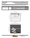
A worst-case estimate, P
D(max)
, represents the maximum allow-
able power level (V
CC(max)
, I
CC(max)
), without exceeding T
J(max)
,
at a selected R
θJA
and T
A
.
Example: Reliability for V
CC
at T
A
=
150°C, package UA, using
minimum-K PCB.
Observe the worst-case ratings for the device, specifi cally:
R
θJA
=
165°C/W, T
J(max)
=
165°C, V
CC(max)
=
5.5 V, and
I
CC(max)
=
8
mA.
Calculate the maximum allowable power level, P
D(max)
. First,
invert equation 3:
ΔT
max
= T
J(max)
– T
A
= 165
°C
–
150
°C = 15
°C
This provides the allowable increase to T
J
resulting from internal
power dissipation. Then, invert equation 2:
P
D(max)
= ΔT
max
÷ R
θJA
= 15°C ÷ 165 °C/W = 91 mW
Finally, invert equation 1 with respect to voltage:
V
CC(est)
= P
D(max)
÷ I
CC(max)
= 91 mW ÷ 8 mA = 11.4 V
The result indicates that, at T
A
, the application and device can
dissipate adequate amounts of heat at voltages ≤V
CC(est)
.
Compare V
CC(est)
to V
CC(max)
. If V
CC(est)
≤ V
CC(max)
, then reli-
able operation between V
CC(est)
and V
CC(max)
requires enhanced
R
θJA
. If V
CC(est)
≥ V
CC(max)
, then operation between V
CC(est)
and
V
CC(max)
is reliable under these conditions.