


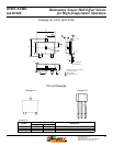
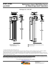
Ratiometric Linear Hall Effect Sensor
for High-Temperature Operation
A1321, A1322,
and A1323
8
Allegro MicroSystems, Inc.
115 Northeast Cutoff
Worcester, Massachusetts 01615-0036 U.S.A.
1.508.853.5000; www.allegromicro.com
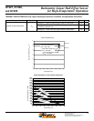
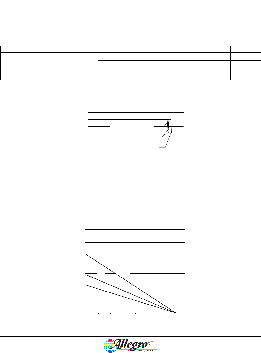
THERMAL CHARACTERISTICS may require derating at maximum conditions, see application information
Characteristic Symbol Test Conditions* Value Units
Package Thermal Resistance
R
θJA
Package LH, 1-layer PCB with copper limited to solder pads 228 ºC/W
Package LH, 2-layer PCB with 0.463 in.
2
of copper area each side
connected by thermal vias
110 ºC/W
Package UA, 1-layer PCB with copper limited to solder pads 165 ºC/W
*Additional thermal information available on Allegro website.
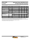
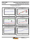
6
5
4
3
2
1
0
20 40 60 80 100 120 140 160 180
Temperature (ºC)
Maximum Allowable V
CC
(V)
Power Derating Curve
(R
QJA
= 228 ºC/W)
1-layer PCB, Package LH
(R
QJA
= 110 ºC/W)
2-layer PCB, Package LH
(R
QJA
= 165 ºC/W)
1-layer PCB, Package UA
V
CC(min)
V
CC(max)
0
100
200
300
400
500
600
700
800
900
1000
1100
1200
1300
1400
1500
1600
1700
1800
1900
20 40 60 80 100 120 140 160 180
Temperature (°C)
Power Dissipation, P
D
(mW)
Power Dissipation versus Ambient Temperature
(R
QJA
= 165 ºC/W)
1-layer PCB, Package UA
(R
QJA
= 228 ºC/W)
1-layer PCB, Packag
e LH
(R
QJA
= 110 ºC/W
)
2-layer PCB, Package LH