www.ti.com
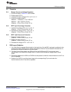
PCB Layout Guideline
2.4 Procedure
2.4.1 Charger Current and Voltage Regulation
1. Ensure that steps in Section 2.3 are followed.
2. Enable output of PS 1.
3. Increase the output voltage of PS 1 to 5 V ±0.1 V.
4. Enable the output of load 2.
Measure → V(J2(OUT)) = 3.6 V ±200 mV
Measure → Ibat = 560 mA ±70 mA
Observe → D2 on, D3 on, D6 off, D7 on.
2.4.2 CFET Input Overvoltage Protection
1. Increase the voltage of PS 1 to 11 V ±0.1 V.
Observe → D2 on, D3 off, D6 off, D7 off.
2. Decrease the voltage of PS 1 to 5 V ±0.1 V.
Observe → D2 on, D3 on, D6 off, D7 on.
2.4.3 CFET Load Overcurrent Protection
1. Enable the output of load 1.
Observe → D2 on, D3 off, D6 off, D7 off.
2. Disable the output of load 1.
Observe → D2 on, D3 on, D6 off, D7 on.
3. Decrease the voltage of PS 1 to 0 V ±0.1 V.
3 PCB Layout Guideline
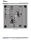
1. It is critical that the exposed thermal pad on the back side of the bq24351 package be soldered to the
printed-circuit board (PCB) ground. Ensure that sufficient thermal vias are located underneath the IC,
connecting to the ground plane on the other layers.
2. The high-current charge paths into ACIN and from the CHGIN and OUT pins must be sized
appropriately for the maximum charge current in order to avoid excessive voltage drops in these
traces.
3. Decoupling capacitors for ACIN and CHGIN must be placed to make the interconnections to the IC as
short as possible.
4. Resistors for VBAT pin must be placed close to the corresponding IC pins and make the
interconnections to the IC as short as possible.
5
SLUU455–October 2010 bq24351EVM for Li-Ion Charger Front-End Protection IC
Submit Documentation Feedback
Copyright © 2010, Texas Instruments Incorporated


