


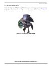


Block Diagram
Variable Speed DC Fan Control using the MC9RS08KA2, Rev. 0
Freescale Semiconductor 15
Chapter 3
Implementation
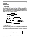
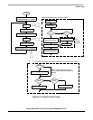
3.1 Block Diagram
The block diagram of the DC fan design is illustrated in Figure 3-1. A 12V low cost bi-phase BLDC motor
is used in this application. The MCU performs alternate outputs to the two NPN transistors that drive the
motor coils. Open drain output Hall sensor is required and positioned close the rotor. The device responds
to magnetic field changes during the motor operation, digitizing output feedback of the rotor position to
the MCU for close loop motor control and fault detection. Ambient temperature information is measured
from an external temperature sensor. In the faulty situation, such as motor jam, the buzzer alarm is driven
by the MCU through a pulse width modulated (PWM) output.
Figure 3-1. DC Fan Design Block Diagram
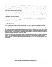
3.2 Hardware Resources
In this application, the low cost MC9RS08KA2 MCU is used. The device has a built-in 8-bit modulo timer
which is used to control the timing for the PWM drive. Bus frequency is chosen to be 4MHz. The design
target for the maximum motor speed is 4000 rpm, the timer must have enough resolution to measure the
shortest PWM period that is less the 3.75ms per commutation step. Timer prescalar is selected as 256
and the timer resolution becomes 64µs.
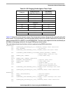
Table 3-1. Hardware Configuration
Bus Frequency 4MHz
Timer Clock for motor speed monitoring 4MHz/256 = 16kHz
Timer Resolution 64µs
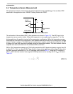
BI-PHASE
MOTOR
HALL
VOLTAGE
REGULATION
12V
+
–
TEMP
SENSOR
RC
BUZZER
MC9RS08KA2
VDD
L1
L2
PTA2
PTA4
PTA5
PTA3
ACMP+
ACMP–