Using the Dual 28V Input Voltage Charger with Linear Regulator, Rev. 1.0
6 Freescale Semiconductor
Layout Design
6 Layout Design
6.1 Layout
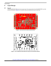
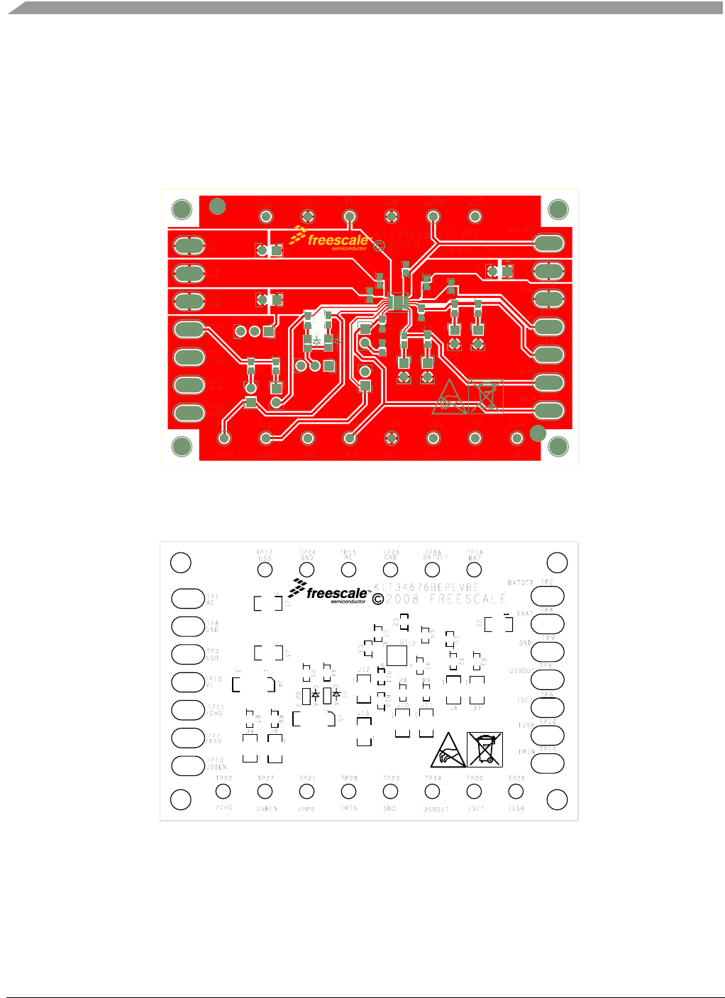
The KIT34676EPEVBE PCB board has two copper layers. The component side of the KIT34676EPEVBE is provided
to locate all components.
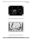
Figure 4 is an overview of the board, followed by the layout of each layer.
Figure 4. The Overview of the Evaluation Board
Figure 5. The Component Side Silkscreen Layer of the Evaluation Board


