Using the Dual 28V Input Voltage Charger with Linear Regulator, Rev. 1.0
8 Freescale Semiconductor
Layout Design
6.2 Layout considerations
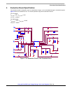
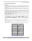
• Place decoupling capacitors C1, C3 and C4 as close as possible to the AC pin, USB pin and BAT pin respectively.
• Place the charge current setting resistor as close as possible to the current setting pin to minimize the parasitic
capacitance between the current setting pin and ground.
• Use wide traces to connect input power source to the AC pin and USB pin, and BAT pin to the battery.
• To get better thermal performance, put the EPAD pin of the MC34676B on a large ground plane on the component
side, and use a via array to connect the EPAD pin to the ground layer, or the large ground plane on the other layer.


