


S3F84P4_AN_REV0.00 (PRELIMINARY SPEC) 2 HARDWARE IMPLEMENTATION
2 HARDWARE IMPLEMENTATION
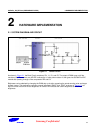
2.1 SYSTEM DIAGRAM AND CIRCUIT
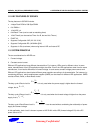
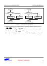
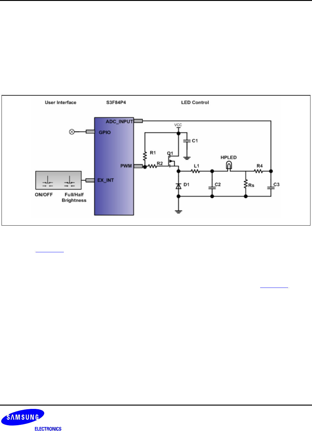
Figure 2-1 Control Circuit
As shown in Figure
2-1, the Buck Circuit comprise of Q1, L1, D1, and C2. The output of PWM turns on/off the
transistor (Q1). The current over HPLED is sensed by a 1ohm power resistor. It then goes into S3F84P4’s ADC
module after passing through a filter composed of R4 and C3.
Brightness can be obtained by changing the PWM duty cycle after comparing the actual sensing value and target
forward current. This application uses two external interrupts (“ENINT” and “GPIO” as shown in Figure
2-1) as
keys to control the turn-on/off and brightness. A normal LED indicates the current brightness as full or half
brightness.
S
amsun
g
Con
f
idential
11