


– 20 –
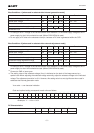
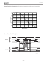
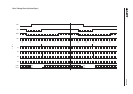
ICX418ALB
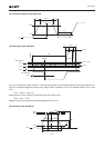
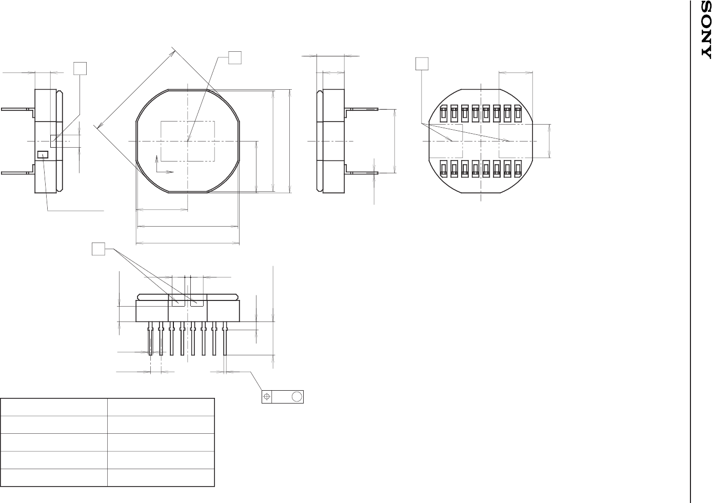
Package Outline Unit: mm
Sony Corporation
16 pin DIP (300mil)
1st. pin Index
H
V
6.175
12.0 ± 0.15
12.35 ± 0.3
φ13.2 ± 0.3
1.84
1.5
1.5
0.71.5
3.29 ± 0.3
2.54
7.62
0.25
4.0
4.0
4.0 ± 0.2
1.0
0.3
1.27
0.6
1.84
1
8
9
16
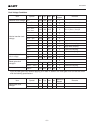
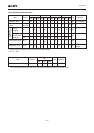
6.175
12.0 ± 0.15
12.35 ± 0.3
8
1
16
9
0.3
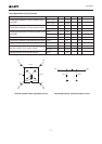
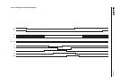
C
~
~
A
B
~
B'
~~
M
1. “A” is the center of the effective image area.
2. The point “B” of the package is the horizontal reference.
The point “B'” of the package is the vertical reference.
3. The bottom “C” of the package is the height reference.
4. The center of the effective image area relative to the center of the package (∗)
is (H, V) = (0, 0) ± 0.15mm.
5. The rotation angle of the effective image area relative to H and V is ± 1˚.
6. The height from the bottom “C” to the effective image area is 1.41 ± 0.15mm.
7. The tilt of the effective image area relative to the bottom “C” is less than 60µm.
8. The thickness of the cover glass is 0.75mm, and the refractive index is 1.5.
∗ Center of the package : The center is halfway between two pairs of opposite sides,
as measured from “B”, “B'”.
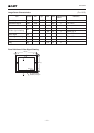
Ceramic
GOLD PLATING
42 ALLOY
PACKAGE STRUCTURE
PACKAGE MATERIAL
LEAD TREATMENT
LEAD MATERIAL
PACKAGE MASS
0.90g
DRAWING NUMBER
AS-B4-01(E)