– 6 –
ICX418ALB
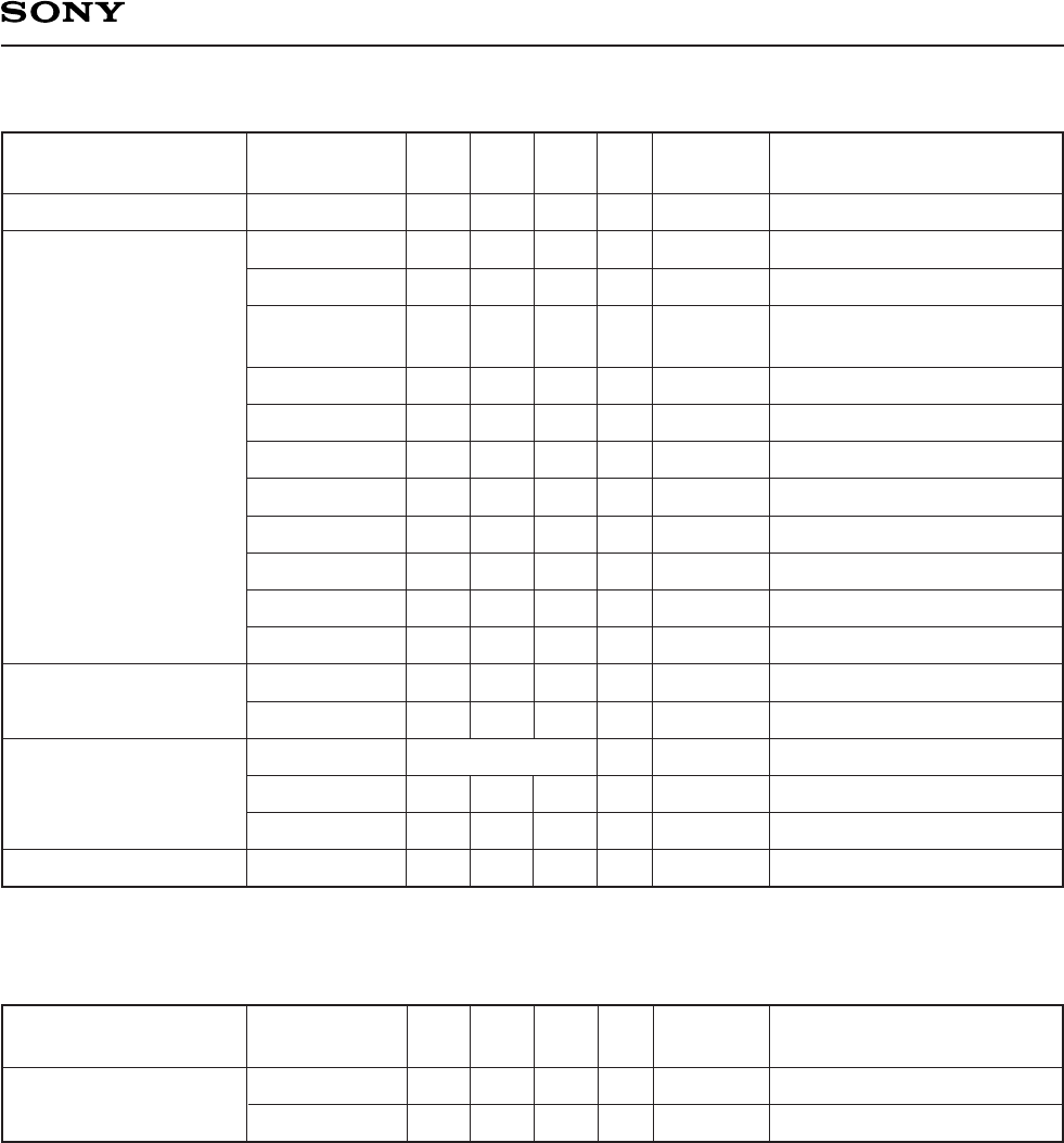
Clock Voltage Conditions
∗1
Input the reset gate clock without applying a DC bias. In addition, the reset gate clock can also be driven
with the following specifications.
Readout clock voltage
Vertical transfer clock
voltage
Horizontal transfer
clock voltage
Reset gate clock
voltage
∗1
Substrate clock voltage
Item
VVT
VVH1, VVH2
VVH3, VVH4
VVL1, VVL2,
VVL3, VVL4
VφV
| VVH1 – VVH2 |
VVH3 – VVH
VVH4 – VVH
VVHH
VVHL
VVLH
VVLL
VφH
VHL
VRGL
VφRG
VRGLH – VRGLL
VφSUB
Symbol
14.55
–0.05
–0.2
–9.6
8.3
–0.25
–0.25
4.75
–0.05
4.5
23.0
Min.
1
2
2
2
2
2
2
2
2
2
2
2
3
3
4
4
4
5
Waveform
diagram
VVH = (VVH1 + VVH2)/2
VVL = (VVL3 + VVL4)/2
VφV = VVHn – VVLn (n = 1 to 4)
High-level coupling
High-level coupling
Low-level coupling
Low-level coupling
Low-level coupling
Remarks
Reset gate clock
voltage
Item
VRGL
VφRG
Symbol
4
4
Waveform
diagram
Remarks
15.0
0
0
–9.0
9.0
5.0
0
∗
1
5.0
24.0
Typ.
15.45
0.05
0.05
–8.5
9.65
0.1
0.1
0.1
0.5
0.5
0.5
0.5
5.25
0.05
5.5
0.8
25.0
Max. Unit
V
V
V
V
Vp-p
V
V
V
V
V
V
V
Vp-p
V
V
Vp-p
V
Vp-p
–0.2
8.5
Min.
0
9.0
Typ.
0.2
9.5
Max. Unit
V
Vp-p


