


– 17 –
ICX423AL
Sony Corporation
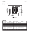
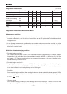
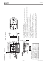
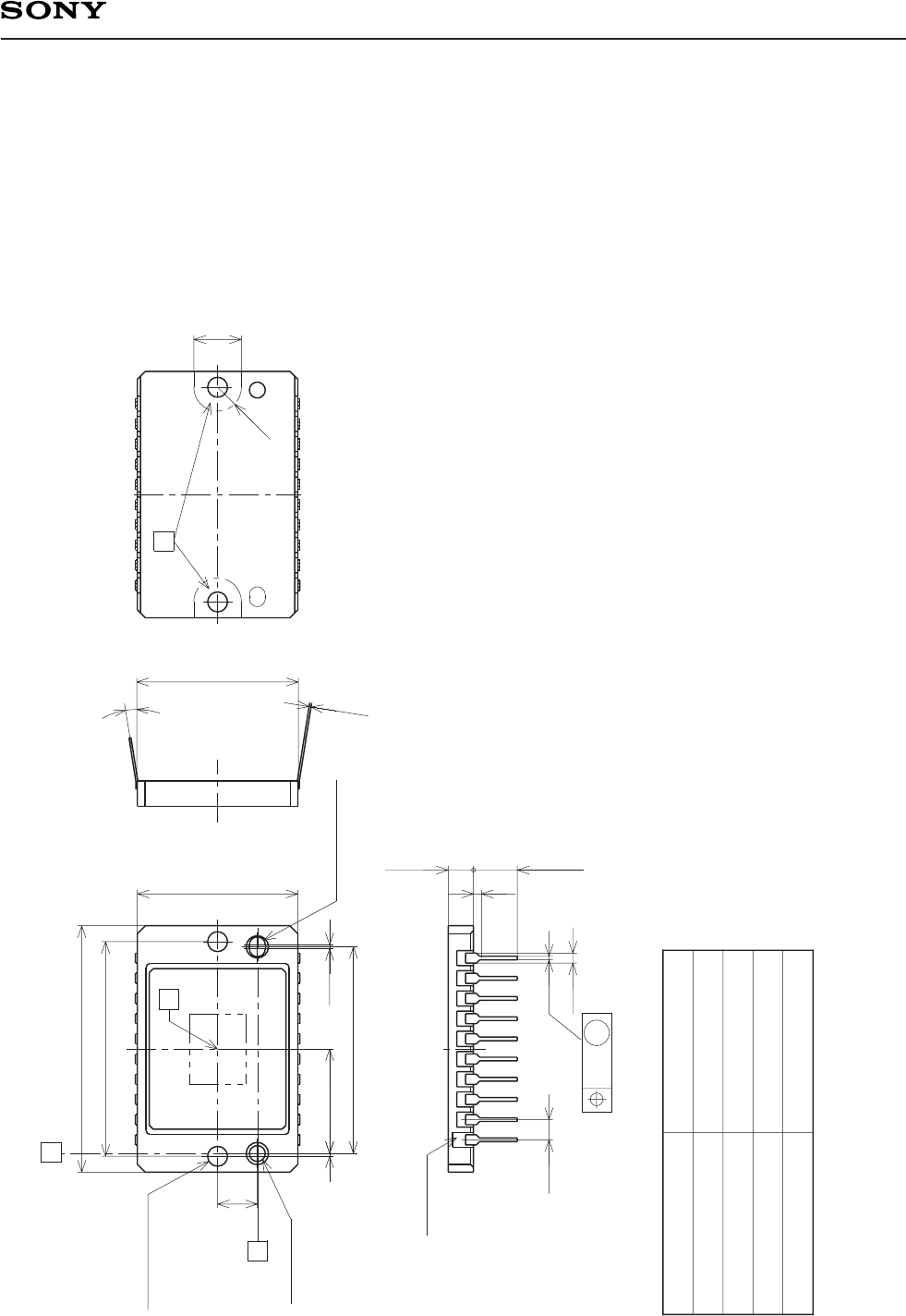
Package Outline Unit: mm
PACKAGE MATERIAL
LEAD TREATMENT
LEAD MATERIAL
PACKAGE MASS
DRAWING NUMBER
Ceramic
GOLD PLATING
5.90g
42 ALLOY
AS-A11(E)
PACKAGE STRUCTURE
M
0.3
0.25
0.35 13.15
5.0
R3.0
6.0
2.54
1.27
0.46
5.5 ± 0.2
26.0 ± 0.25
3.2 ± 0.3
20.32
20.2 ± 0.3
0.5
1.0
2-
2-
D
A
(AT STAND OFF)
11
20
1
10
31.0 ± 0.4
27.0 ± 0.3
2-φ2.50
+ 0.25
– 0
φ2.00
+ 0.15
– 0
(Reference Hole)
1Pin Index
(Elongated Hole)
2.00
+ 0.15
– 0
×2.5
C
B
0˚ to 9˚
~
~
20 pin DIP (800mil)
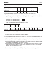
1.
"
A
"
is the center of the effective image area.
2
.
The straight line “B” which passes through the center of the reference hole and the elongated
hole is the reference axis of vertical direction (V).
3
.
The straight line “C” which passes through the center of the reference hole at right angle to vertical
reference line “B” is the reference axis of horizontal direction (H).
4
.
The bottom “D” is the height reference.(Two points are specified.)
5. The center of the effective image area specified relative to the reference hole
is (H, V) = (13.15, 5.0) ± 0.15mm.
6
.
The angle of rotation relative to the reference line “B” is less than ± 1˚
7
.
The height from the bottom “D” to the effective image area is 1.46 ± 0.15mm.
8
.
The tilt of the effective image area relative to the bottom “D” is less than 60µm.
9
.
The thickness of the cover glass is 0.75mm and the refractive index is 1.5.