


– 5 –
ICX423AL
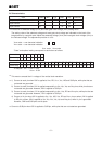
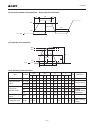
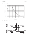
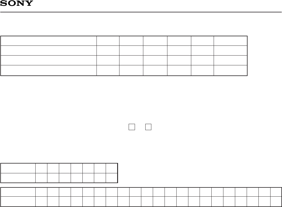
DC Characteristics
Output amplifier drain current
Input current
Input current
Item
IDD
IIN1
IIN2
Symbol
6
Min. Unit RemarksTyp. Max.
mA
µA
µA
1
10
∗
2
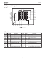
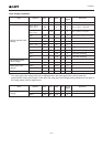
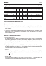
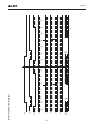
Indications of substrate voltage (VSUB) and reset gate clock voltage (VRGL) setting value
The setting value of the substrate voltage and reset gate clock voltage are indicated on the back of the
image sensor by a special code. Adjust the substrate voltage (VSUB) and reset gate clock voltage (VRGL) to
the indicated voltage. The adjustment precision is ±3%.
VSUB code — one character indication
VRGL code — one character indication ↑↑
VRGL code VSUB code
"Code" and optimal setting correspond to each other as follows.
<Example> "5K" → VRGL = 2.0V
VSUB = 12.0V
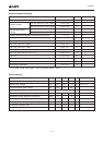
VSUB code
Optimal setting
D
9.0
∗
4
∗
5
E
9.5
f
10.0
G
10.5
h
11.0
J
11.5
K
12.0
L
12.5
m
13.0
N
13.5
P
14.0
Q
14.5
R
15.0
S
15.5
T
16.0
U
16.5
V
17.0
W
17.5
X
18.0
Y
18.5
Z
19.0
VRGL code
Optimal setting
1
0
2
0.5
3
1.0
4
1.5
5
2.0
6
2.5
7
3.0
∗
3
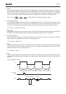
This must no exceed the VVL voltage of the vertical clock waveform.
∗
4
1) Current to each pin when 20V is applied to VDD, RD, VOUT, VSS, HIS and SUB pins, while pins that are
not tested are grounded.
2) Current to each pin when 20V is applied sequentially to Vφ1, Vφ2, Vφ3 and Vφ4 pins, while pins that are
not tested are grounded. However, 20V is applied to SUB pin.
3) Current to each pin when 15V is applied sequentially to Hφ1, Hφ2, RG and VGG pins, while pins that are
not tested are grounded. However, 15V is applied to SUB pin.
4) Current to VL pin when 30V is applied to Vφ1, Vφ3, HIS, VDD, RD and VOUT pins or when, 24V is applied
to RG pin or when, 20V is applied to Vφ2, Vφ4, VGG, VSS, Hφ1 and Hφ2 pins, while VL pin is grounded.
However, GND and SUB pins are left open.
∗
5
Current to SUB pin when 55V is applied to SUB pin, while pins that are not tested are grounded.