


– 6 –
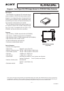
ICX423AL
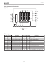
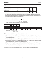
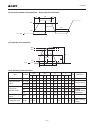
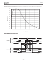
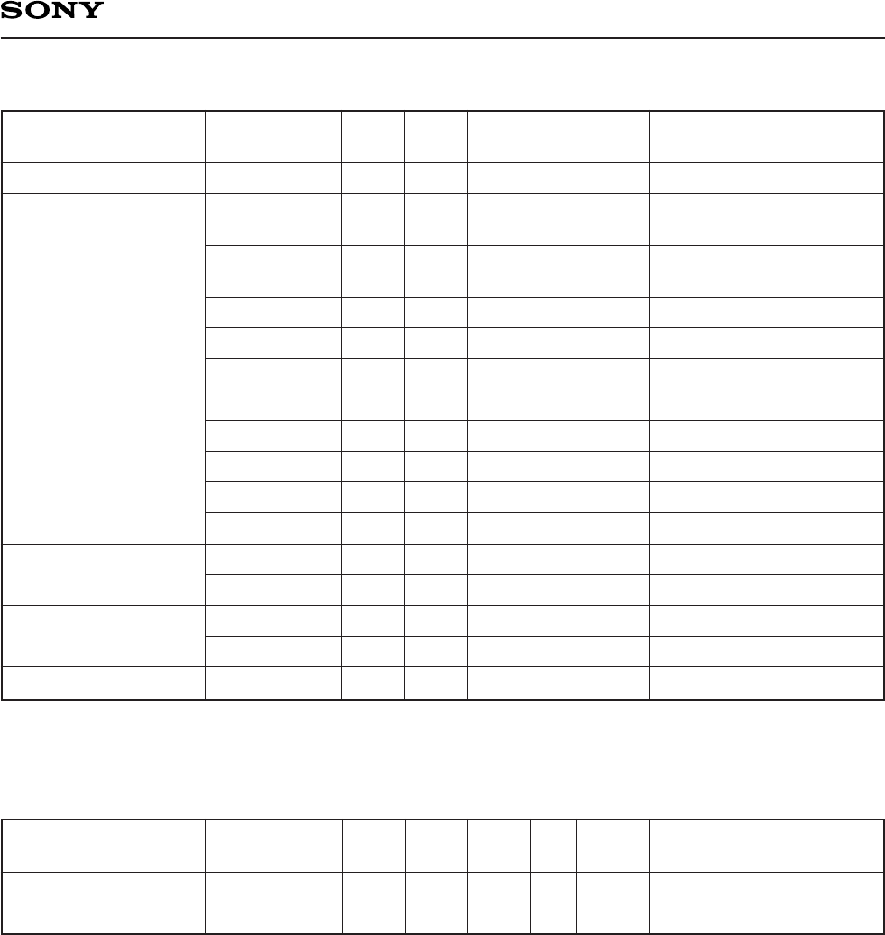
Clock Voltage Conditions
∗
1
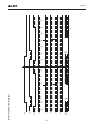
The reset gate clock voltage need not be adjusted when the reset gate clock is driven when the
specifications are as given below. In this case, the reset gate clock voltage setting indicated on the back of
the image sensor has not significance.
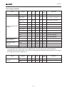
Readout clock voltage
Vertical transfer clock
voltage
Horizontal transfer
clock voltage
Reset gata clock
voltage
Substrate clock voltage
Item
VVT
VVH1, VVH2,
VVH3, VVH4
VVL1, VVL2,
VVL3, VVL4
VφV
| VVH1 – VVH2 |
VVH3 – VVH
VVH4 – VVH
VVHH
VVHL
VVLH
VVLL
VφH
VHL
VφRG
VRGL
VφSUB
Symbol
14.5
–0.6
8.9
–0.5
–0.5
6.0
–3.5
6.0
0
27.0
Min.
15.0
–9.6
Typ.
15.5
0
0.2
0
0
0.8
1.0
0.8
0.8
8.0
–3.0
13.0
3.0
32.0
Max. Unit
1
2
2
2
2
2
2
2
2
2
2
3
3
3
3
4
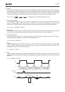
Waveform
diagram
VVH = (VVH1 + VVH2)/2
VVL = (VVL3 + VVL4)/2
VφV = VVHn – VVLn (n = 1 to 4)
High-level coupling
High-level coupling
Low-level coupling
Low-level coupling
∗
1
Remarks
V
V
V
V
V
V
V
V
V
V
V
V
V
V
V
V
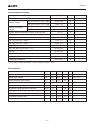
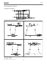
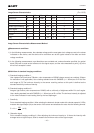
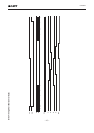
Reset gate clock
voltage
Item
VRGL
VφRG
Symbol
–0.2
8.5
Min.
0
9.0
Typ.
0.2
9.5
Max. Unit
3
3
Waveform
diagram
Remarks
V
V