40
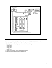
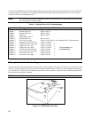
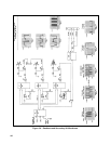
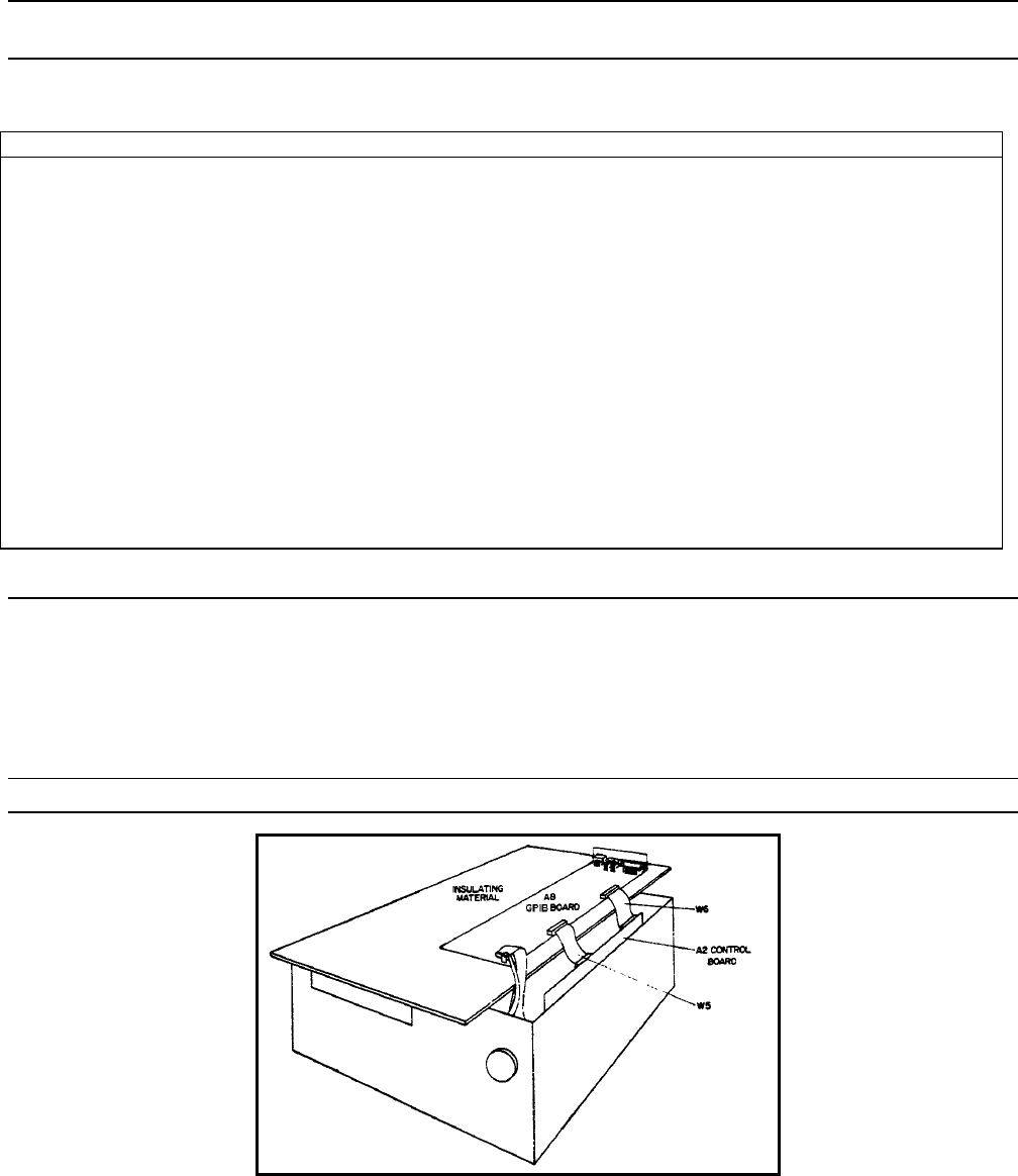
To remove the GPIB board, perform the GPIB board removal procedure discussed earlier in this section. Lay out the board
as shown in Figure 3-2 with a piece of insulating material under the board. Reconnect connectors W1, W2, W5, and W6
after the board is on the insulating material.
Note: The GPIB board can be placed alongside the unit for troubleshooting by using extender cables provided in
service kit Agilent P/N 06033-60005.
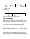
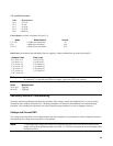
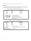
Table 3-1. Selftest Error Code Troubleshooting
Error Code Description Check Functional Circuit
ERROR 4 External RAM Test Replace A8U8
ERROR 5 Internal RAM Test Replace A8U14
ERROR 6 External ROM Test Replace A8U6
ERROR 7 GPIB Test Replace A8U17
ERROR 8 GPIB address set to 31
ERROR 10 Internal ROM Test Replace A8U4
ERROR 12 ADC Zero Too High Check U11,20,24,66,67; go to Readback DAC Troubleshooting
ERROR 13 Voltage DAC Full Scale Low Check U2,7,64,69
ERROR 14 Voltage DAC Full Scale High Check U2,7,64,69
ERROR 15 Voltage DAC Zero Low Check U2,7,64,69
ERROR 16 Voltage DAC Zero High Check U2,7,64,69
ERROR 17 Current DAC Full Scale Low Check U9,65,68
ERROR 18 Current DAC Full Scale High Check U9,65,68
ERROR 19 Current DAC Zero Low Check U9,65,68
ERROR 20 Current DAC Zero High Check U9,65,68
┐
│
│
│
├─
│
│
│
┘
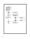
Go to Secondary SA
Troubleshooting
Primary Interface Troubleshooting
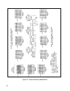
Primary interface troubleshooting checks for the presence of bias voltages, clock signals (see Figure 3-3), and activity on the
data lines. Primary signature analysis may be used to further troubleshoot these circuits, but since the address and data lines
go to so many IC's, it may not be cost-effective to narrow an incorrect signature to a specific chip. GPIB board replacement
may be the most cost-effective solution.
Note: The initialization procedure in Page 31 must be performed when the GPIB board is replaced.
Figure 3-2. GPIB Board Test Setup


