


USQ Series
4
Removal of Soldered USQ's from PCB's
Should removal of the USQ from its soldered connection be needed, it is very
important to thoroughly de-solder the pins using solder wicks or de-soldering
tools. At no time should any prying or leverage be used to remove boards that
have not been properly de-soldered first.
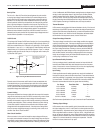
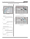
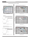
Input Source Impedance
USQ converters must be driven from a low ac-impedance input source.
The DC/DC’s performance and stability can be compromised by the use of
highly inductive source impedances. The input circuit shown in Figure 2 is a
practical solution that can be used to minimize the effects of inductance in
the input traces. For optimum performance, components should be mounted
close to the DC/DC converter. The 24V models can benefit by increasing
the 33µF external input capacitors to 100µF, if the application has a high
source impedance.
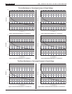
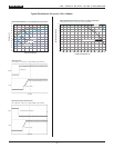
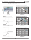
I/O Filtering, Input Ripple Current, and Output Noise
All models in the USQ Series are tested/specified for input ripple current (also
called input reflected ripple current) and output noise using the circuits and
layout shown in Figures 2 and 3.
External input capacitors (C
IN in Figure 2) serve primarily as energy-storage
elements. They should be selected for bulk capacitance (at appropriate
frequencies), low ESR, and high rms-ripple-current ratings. The switching
nature of DC/DC converters requires that dc voltage sources have low ac
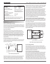
Figure 3. Measuring Output Ripple/Noise (PARD)
Input Overvoltage Shutdown
Standard USQ DC/DC converters do not feature overvoltage shutdown.
They are equipped with this function, however. Many of our customers need
their devices to withstand brief input surges to 100V without shutting down.
Consequently, we disabled the function. Please contact us if you would like it
enabled, at any voltage, for your application.
Start-Up Threshold and Undervoltage Shutdown
Under normal start-up conditions, the USQ Series will not begin to regulate
properly until the ramping input voltage exceeds the Start-Up Threshold.
Once operating, devices will turn off when the applied voltage drops below
the Undervoltage Shutdown point. Devices will remain off as long as the
undervoltage condition continues. Units will automatically re-start when the
applied voltage is brought back above the Start-Up Threshold. The hyster
-
esis built into this function avoids an indeterminate on/off condition at a single
input voltage. See Performance/Functional Specifications table for actual limits.
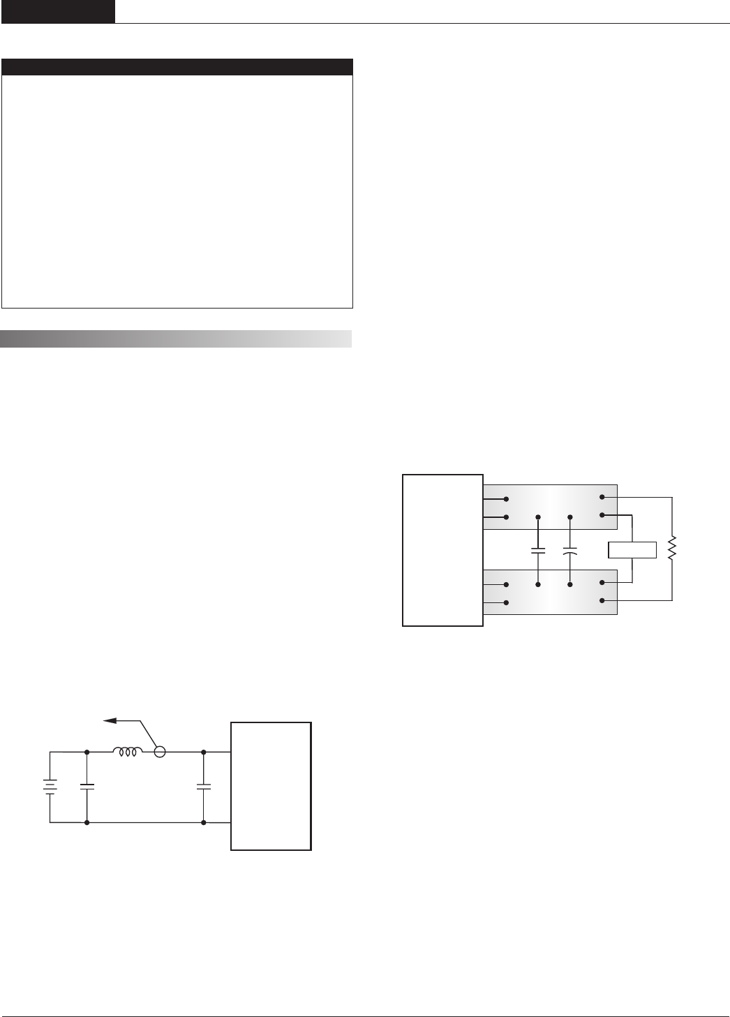
Figure 2. Measuring Input Ripple Current
C
IN
V
IN
C
BUS
L
BUS
C
IN
= 33µF, ESR < 700mΩ @ 100kHz
C
BUS
= 220µF, ESR < 100mΩ @ 100kHz
L
BUS
= 12µH
3
1
+INPUT
–INPUT
CURRENT
PROBE
TO
OSCILLOSCOPE
+
–
C1
C1 = 1µF CERAMI
C
C2 = 10µF
TANTALUM
LOAD 2-3 INCHES (51-76mm) FROM MODULE
C2
R
LOAD
7
8
COPPER STRI
P
4
5
COPPER STRI
P
SCOPE
+OUTPUT
–OUTPUT
+SENSE
–SENSE
T E C H N I C A L N O T E S
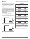
Absolute Maximum Ratings
Input Voltage: 24V models 48V models
Continuous: 39 Volts 81 Volts
Transient (100msec) 50 Volts 100 Volts
Input Reverse-Polarity Protection Input Current must be <5A. 1 minute
duration. Fusing recommended.
Output Current Current limited. Devices can withstand
an indefinite output short circuit.
On/Off Control (Pin 2) Max. Voltages
Referenced to –Input (pin 1) –0.3 to +7 Volts
Storage Temperature –40 to +125°C
Lead Temperature (Soldering, 10 sec.) +300°C
These are stress ratings. Exposure of devices to any of these conditions may adversely
affect long-term reliability. Proper operation under conditions other than those listed in the
Performance/Functional Specifications Table is not implied, nor recommended.
impedance as highly inductive source impedance can affect system stability.
In Figure 2, CBUS and LBUS simulate a typical dc voltage bus. Your specific
system configuration may necessitate additional considerations.
In critical applications, output ripple/noise (also referred to as periodic and
random deviations or PARD) can be reduced below specified limits using
filtering techniques, the simplest of which is the installation of additional
external output capacitors. Output capacitors function as true filter elements
and should be selected for bulk capacitance, low ESR, and appropriate
frequency response. In Figure 3, the two copper strips simulate real-world
pcb impedances between the power supply and its load. Scope measurements
should be made using BNC connectors or the probe ground should be less
than ½ inch and soldered directly to the fixture.
All external capacitors should have appropriate voltage ratings and be
located as close to the converter as possible. Temperature variations for all
relevant parameters should be taken into consideration. OS-CON
TM
organic
semiconductor capacitors (www.sanyo.com) can be especially effective for
further reduction of ripple/noise.
The most effective combination of external I/O capacitors will be a function
of line voltage and source impedance, as well as particular load and layout
conditions. Our Applications Engineers can recommend potential solutions
and discuss the possibility of our modifying a given device’s internal filtering
to meet your specific requirements. Contact our Applications Engineering
Group for additional details.
2 0 A , S I N G L E O U T P U T D C / D C C O N V E R T E R S