


NVIDIA Corporation 33
C
HAPTER 5
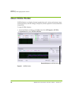
Supplemental Information for the Adjust Motherboard Settings Page
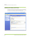
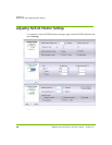
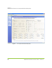
Memory Controller Timing Group
The memory controller timing section lets you control essential timings in order to
maintain stability when overclocking the front side bus and memory bus. Increasing
(relaxing) these parameters should allow for increased margins when performing
overclocking functions.
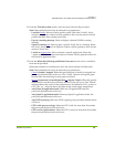
• Row Address Strobe (tRAS)
This is the amount of time between a row being activated by precharge and then
deactivated. The shorter the time, the faster the performance, but if it is set too low,
it can cause data corruption.
• RAS to CAS Access (tRCD)
This is the amount of time, in cycles, between issuing an active command and then
issuing the read/write commands.
• Memory Bank Switch (tRP)
This is the minimum time between active commands and the read/writes of the
next bank on the memory module.
• Row Cycle Time (tRC)
This is the minimum time, in cycles, that it takes a row to complete a full cycle.
This can be determined by tRC = tRAS + tRP. If this is set too low it can cause
corruption of data. If it is too high, it will increase stability but cause a loss in
performance.
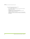
• Write Recovery Time (tWR)
This is the memory timing that determines the delay between a write command
and a precharge command sent to the same bank of memory.
• RAS to RAS Delay (tRRD)
This is the amount of cycles that it takes to activate the next bank of memory. It is
the opposite of tRAS. The lower the timing, the better the performance, but it can
cause instability.
• Read to Write Delay (tRWT)
When a write command is received, this is the amount of cycles for the command
to be executed.