


34 NVIDIA nTune Generation 5.0 User’s Guide – Version 2.0
C
HAPTER 5
Supplemental Information for the Adjust Motherboard Settings Page
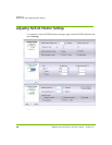
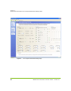
• Write to Read Delay (tWTR)
This is the amount of cycles required between a valid write command and the next
read command. Lower values result in better performance, but can cause
instability.
• Write to Read Time (tWRRD)
This is the number of clock cycles between the last write data pair and the
subsequent READ command to the same physical bank.
• Write to Write Time (tWRWR)
This is the number of clock cycles between the last write and the subsequent
WRITE command to the same physical bank.
• Read to Read Time (tRDRD)
This is the number of clock cycles between the last read and the subsequent READ
command to the same physical bank.
•Refresh Timing (tREF)
This is the amount of time, in microseconds(µs), it takes before a charge is
refreshed so it does not lose its charge and become corrupted.
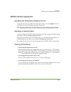
The following settings require a reboot and must be set in the BIOS Setup or using the
Dynamic BIOS Access page if available.
• Command Per Clock (tCPC)
This is the amount of time in cycles between when the chip select is executed and
when the commands can be issued. A lower value (1T) results in faster
performance, but 2T is used to maintain system stability.
•Column Address Strobe (tCAS)
This controls the amount of time in cycles between sending a reading command
and acting on it. From the beginning of the CAS to the end of the CAS is the
latency. The lower the time, in cycles, the higher the memory performance.