Appendix E: Performance Verification
A–22
VX4801 Programmable Digital I/O Module
VX4801 Under-Test Configuration
In order to perform this procedure, the VX4801 under-test must be installed in an
approved VXIbus system. At a minimum, the system must contain the elements
listed in Table 2.
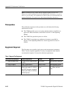
Table 2: Elements of a Minimum VX4801 Under-Test System
Item Number and Description Minimum Requirements Example Purpose
1. VXIbus Mainframe Two available slot for VX4801
under-test and the VX4801 digital
signal source (Slave) in addition to
the Slot 0 controller
Tektronix VX1400A Provides power, cooling, and
backplane for VXIbus modules
2. Slot 0 Controller Resource Mgr., Slot 0 Functions,
IEEE 488 GPIB Interface
VX4521 Slot 0 Resource Mgr. Provides Slot 0 functions.,
Resource Mgr., and GPIB/
VXIbus interface
3. VXIbus System Controller VXIbus-Talker/Listener/Controller IBM 486 PC with National
Instruments GPIB PC2A card
& NI-488.2M software, GPIB
cable (Tektronix P/N
012–0991-00)
Provides VXIbus command
and response interface
4. VX4801 Under-Test Not applicable Not applicable Verify its performance
5. VX4801-Slave 4 byte TTL/CMOS I/O VX4801 Provides test signal I/O
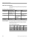
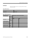
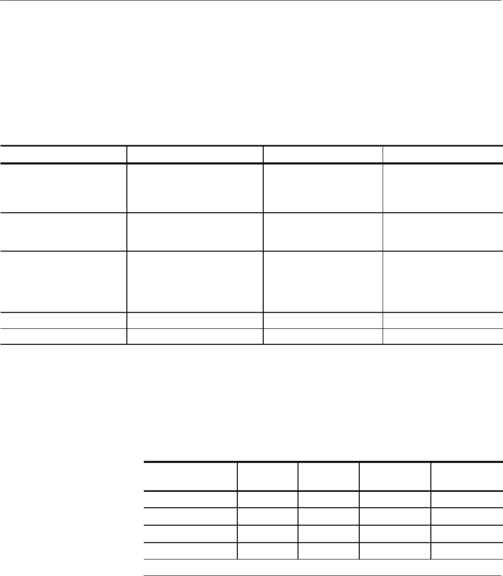
Table 3 describes the VXIbus system configuration assumed in this procedure. If
your configuration is different, you do not need to change it, just note that you
will observe your device names and addresses in test sequences. (Note that no
secondary addressing is assumed.)
Table 3: Test System Configuration (Assumed)
Device
GPIB Device
Name
VXI Slot
VXIbus Logical
Address
GPIB Primary
Address
GPIB0 GPIB0 (PC card) NA 30
VX4521 VX4521 Slot 0 0D (hex) 13
VX4801 under-test VX4801 Slot 1 01 1
VX4801 slave slave Slot 2 02 2
Test System Configuration


