


GE864 Hardware User Guide
1vv0300694 Rev.10 - 10/06/08
Reproduction forbidden without Telit Communications S.p.A. written authorization - All Rights Reserved page 4 of 69
9.2 OUTPUT LINES (Speaker)....................................................................................................42
9.2.1 Short description............................................................................................................................ 42
9.2.2 Output Lines Characteristics.......................................................................................................... 43
9.3 SIM Holder Implementation .................................................................................................43
10 General Purpose I/O.......................................................................................................44
10.1 GPIO Logic levels .................................................................................................................46
10.2 Using a GPIO Pad as INPUT ................................................................................................47
10.3 Using a GPIO Pad as OUTPUT
............................................................................................47
10.4 Using the RF Transmission Control GPIO4
.......................................................................48
10.5 Using the RFTXMON Output GPIO5
....................................................................................48
10.6 Using the Alarm Outpu
t
GPIO6 ...........................................................................................48
10.7 Using the Buzzer Output GPIO7..........................................................................................49
10.8 Magnetic Buzzer Concepts
..................................................................................................50
10.8.1 Short Description ........................................................................................................................... 50
10.8.2 Frequency Behaviour..................................................................................................................... 51
10.8.3 Power Supply Influence................................................................................................................. 51
10.8.4 Warning.......................................................................................................................................... 51
10.8.5 Working Current Influence............................................................................................................. 51
10.9 Using the Temperature Monitor Function ..........................................................................52
10.9.1 Short Description ........................................................................................................................... 52
10.9.2 Allowed GPIO ................................................................................................................................ 52
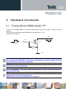
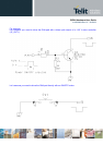
10.10 Indication of network service availability .......................................................................53
10.11 RTC Bypas
s out ................................................................................................................54
10.12 VAUX1 pow
er output ........................................................................................................54
11 DAC and ADC section....................................................................................................55
11.1 DAC Converter......................................................................................................................55
11.1.1 Description..................................................................................................................................... 55
11.1.2 Enabling DAC ................................................................................................................................ 56
11.1.3 Low Pass Filter Example ............................................................................................................... 56
11.2 ADC Converter......................................................................................................................57
11.2.1 Description..................................................................................................................................... 57
11.2.2 Using ADC Converter .................................................................................................................... 57
12 Mounting the GE864 on your Board .............................................................................58
12.1 General ..................................................................................................................................58
12.1.1 Module finishing & dimensions...................................................................................................... 58
12.1.2 Recommended foot print for the application (GE864)................................................................... 59
12.1.3 Suggested Inhibit Area .................................................................................................................. 60
12.1.4 Debug of the GE864 in production ................................................................................................ 61
12.1.5 Stencil ............................................................................................................................................ 61
12.1.6 PCB pad design............................................................................................................................. 62