


Performance Tests
1–28
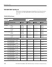
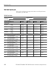
TDS 500D, TDS 600B & TDS 700D Performance Verification and Specifications
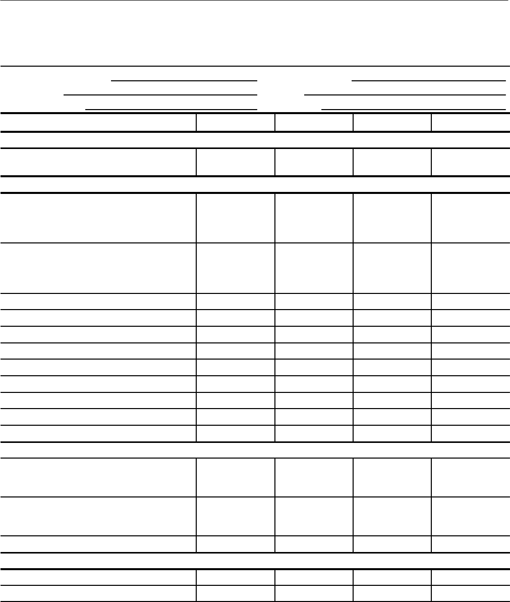
TDS 794D Test Record (cont.)
Instrument Serial Number: Certificate Number:
Temperature: RH %:
Date of Calibration: Technician:
TDS 794D Performance Test MaximumOutgoingIncomingMinimum
Time Base System
Long Term Sample Rate/
Delay Time @ 100 ns/10.0 ms
–2.5 Div __________ __________ +2.5 Div
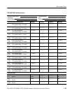
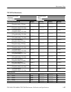
Trigger System Accuracy
Pulse-Glitch or Pulse-Width,
Hor. scale ≤ 1 ms
Lower Limit
Upper Limit
3.5 ns
3.5 ns
__________
__________
__________
__________
6.5 ns
6.5 ns
Pulse-Glitch or Pulse-Width,
Hor. scale > 1 ms
Lower Limit
Upper Limit
1.9 ms
1.9 ms
__________
__________
__________
__________
2.1 ms
2.1 ms
Main Trigger, DC Coupled, Positive Slope 4.8953 V __________ __________ 5.1047 V
Main Trigger, DC Coupled, Negative Slope 4.8953 V __________ __________ 5.1047 V
Delayed Trigger, DC Coupled, Positive Slope 4.8953 V __________ __________ 5.1047 V
Delayed Trigger, DC Coupled, Negative Slope 4.8953 V __________ __________ 5.1047 V
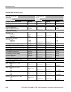
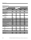
CH1 Sensitivity, 50 MHz, Main Pass/Fail __________ __________ Pass/Fail
CH1 Sensitivity, 50 MHz, Delayed Pass/Fail __________ __________ Pass/Fail
CH1 AUX Trigger Input Pass/Fail __________ __________ Pass/Fail
CH1 Sensitivity, full bandwidth, Main Pass/Fail __________ __________ Pass/Fail
CH1 Sensitivity, full bandwidth, Delayed Pass/Fail __________ __________ Pass/Fail
Output Signal Checks
MAIN TRIGGER OUTPUT, 50 W
High
Low
High ≥ 1.0 V __________
__________
__________
__________
Low ≤ 0.25 V
DELAYED TRIGGER OUTPUT, 50 W
High
Low
High ≥ 1.0 V __________
__________
__________
__________
Low ≤ 0.25 V
CH 3 SIGNAL OUTPUT, 50 W Pk-Pk ≥ 44 mV __________ __________ Pk-Pk ≤ 66 mV
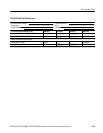
Probe Compensator Output Signal
Frequency (CH1 Freq). 950 Hz __________ __________ 1.050 kHz
Voltage (difference) 495 mV __________ __________ 505 mV