


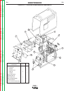
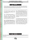

V300-I
THEORY OF OPERATION
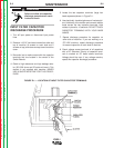
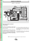
PRECHARGE & PROTECTION CIRCUITS
The DC voltage from the Input Rectifier is applied to the
Driver Board to begin charging the Switch Board
capacitors at a slow rate. When the pre-charge level is
achieved, the input relays close, applying the full DC
voltage to the capacitors. Depending on the Code
Number of the machine, there will be either two or four
relays and they may or may not be mounted on the
Driver Board.
The Driver Board is also responsible for gating the
Field Effect Transistors (FETs) on the Switch Boards,
as directed by the pulse width modulated (PWM) signal
from the Control Board.
The Protection Board monitors the capacitors for prop-
er balance and voltage level. If an imbalance or over-
voltage condition is detected, the Protection Circuit will
de-energize the relays, removing the power from the
switch circuits. The machine output will also be dis-
abled.
Another function of the Protection Board is to detect
whether the input voltage is single phase or three
phase and pass that information to the Control Board.
The maximum output of the machine will be limited to
approximately 250 amps with single phase input and
360 amps with 3 phase input.
E-3 E-3
Return to Section TOC Return to Section TOC Return to Section TOC Return to Section TOC
Return to Master TOC Return to Master TOC Return to Master TOC Return to Master TOC
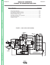
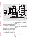
FIGURE E-3 ---PRECHARGE & PROTECTION CIRCUITS
1ø OR 3ø DETETCTION (H5)
LINE
SWITCH
INPUT
RECTIFIER
AC1
AC2
AC3
A-LEAD
AUXILIARY
TRANSFORMER
TO
WIREFEEDER
18VAC
24VAC
POWERBOARD
24VDC
PRE-CHARGE
2ND STEP PWM
1ST STEP PWM VOLTAGE
15VDC-CONTROL BOARD FUNCTION VOLTAGE
24VAC-THERMOSTATS-GUN TRIGGERING
LOCAL
REMOTE
METER
MODE
POT
POT
<1 VDC
FAN
1
2
3
CONTROL
BOARD
Y-Y FEEDBACK
3A
POWER SWITCH
SECTIONS
20KHZ
CURRENT
TRANSFORMER
MAIN
TRANSFORMER
CHOKE
RECTIFIER
HEATSINK
BOTTOM
1 DIODE
5 DIODES
5 DIODES
TOP
TOP
1 DIODE
CHOKE
CHOKE
SHUNT
CURRENT FEEDBACK-PROTECTION
VOLTA GE FEEDBACK
PULSE
TRAIN
DRIVER
BOARD
PRE-CHARGE
CR1
CR2
LEFT SWITCH BOARD
FET MODULES
CAP
FET MODULES
RIGHT SWITCH BOARD
FET MODULES
CAP
FET MODULES
PROTECTION
BOARD
NOTE: Unshaded areas of block logic diagram are the subject of discussion