


V300-I
THEORY OF OPERATION
E-7 E-7
Return to Section TOC Return to Section TOC Return to Section TOC Return to Section TOC
Return to Master TOC Return to Master TOC Return to Master TOC Return to Master TOC
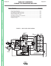
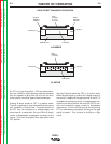
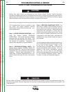
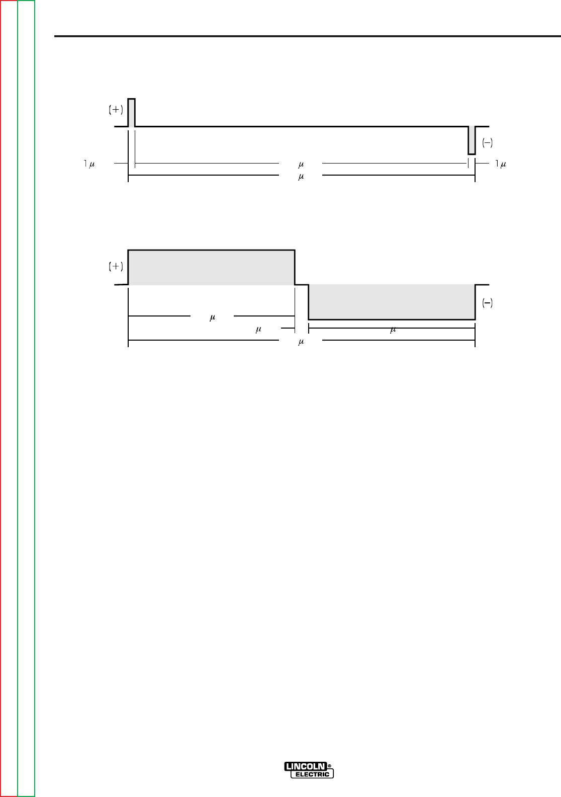
Since only 2 microseconds of the 50-microsecond
time period is devoted to conducting, the output
power is minimized.
MAXIMUM OUTPUT
By holding the gate signals on for 24 microseconds
each and allowing only 2 microseconds of dwell time
(off time) during the 50-microsecond cycle, the output
is maximized. The darkened area under the top
curve can be compared to the area under the bottom
curve. The more dark area under the curve, the
more power is present.
The term PULSE WIDTH MODULATION is used to
describe how much time is devoted to conduction in
the positive and negative portions of the cycle.
Changing the pulse width is known as MODULA-
TION. Pulse Width Modulation (PWM) is the varying
of the pulse width over the allowed range of a cycle
to affect the output of the machine.
MINIMUM OUTPUT
By controlling the duration of the gate signal, the FET
is turned on and off for different durations during a
cycle. The top drawing above shows the minimum
output signal possible over a 50-microsecond time
period.
The positive portion of the signal represents one FET
group
1
conducting for 1 microsecond. The negative
portion is the other FET group
1
. The dwell time (off
time) is 48 microseconds (both FET groups off).
FIGURE E.6 — TYPICAL FET OUTPUTS.
MINIMUM OUTPUT
MAXIMUM OUTPUT
24
50
24
2
48
50
sec
sec
sec
sec
sec
sec
sec
sec
PULSE WIDTH MODULATION
1
An FET group consists of the sets of FET modules grouped
onto one switch board.