


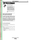
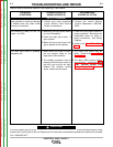

THEORY OF OPERATION
E-3 E-3
INVERTEC® V205-T AC/DC™
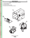
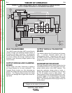
MAIN IGBT INVERTER BOARD
The filtered input voltage, from the Input Board, is
applied through an input choke to the Main IGBT
Inverter Board. This input voltage is rectified, regulat-
ed and a unity power factor output is developed for the
main welding IGBTs. This unity power factor circuit
provides several advantages over a traditional bridge
rectifier circuit. Among these advantages are that the
UPFR operates over a wide range of voltages, there is
no need for any manual circuit changes when the input
voltages are changed from 115VAC to 230VAC and
there is absolute voltage stability maintained on the
IGBT electrolytic capacitors. The four main welding
IGBTs are located on a large center mounted heat sink
assembly.
The pre-charge and auto reconnect circuits are posi-
tioned on the Main IGBT Inverter Board. When power
is first applied to the V205T the rectified DC input volt-
age is applied to the input capacitors through a current
limiting circuit. The capacitors are charged slowly and
current limited for approximately five seconds. After
five seconds a relay closes and the pre-charge circuit
is bypassed and a controlled DC input voltage is
applied to the weld capacitors and IGBTs making them
ready for welding output demands when the IGBTs are
gated on. The auto reconnect circuit receives and
processes a low-level voltage signal from the Bus
Board. This low level signal is utilized to adjust for the
FIGURE E.3 - MAIN IGBT INVERTER BOARD
different voltage requirements needed by the weld
IGBT circuits. A signal is also sent to the Control Board
so that when the input voltage is reduced the output of
the machine will be limited accordingly.
The Auxiliary power portion of the board generates
several voltages through flyback topology and a
50KHZ switching frequency. These various voltages
(+24, +15, +5, +48 and –15) are utilized to operate the
control and protection electronics, the gas solenoid,
the trigger circuit and the fan motor.
The Main IGBT Inverter Board receives command and
pre-set signals from the Control/Display board. It also
receives feedback information, both voltage and cur-
rent, from the Output Filter Board and Hall Effect
Device via the Bus Board. It processes this informa-
tion and generates the correct pulse width modulation
signal (PWM) that is applied to the gates of the weld
IGBTs. This controls and regulates the output of the
machine. The thermostats signals are connected to the
Main IGBT Inverter Board. This status information is
passed on to the Control Board. In the case of an over
temperature condition the Control Board will prevent
output until the machine cools and the thermostats
reset.
Low-level analog signals are generated on the Main
IGBT Inverter Board and sent to the Control/Display
Board for meter set and actual display values.
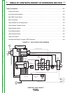
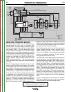
NOTE: Unshaded areas of Block Logic
Diagram are the subject of discussion
Superimposition
board
Bus board
Fan
Input
board
HF
board
Main IGBT
& Power board
4
IGBT's
Control board
Display & LED
board
888
Control
Knob
Gas
Solenoid
DC blocking
capacitor board
Main
Transformer
Output
board
Output
Transistor
Module
Current
Hall
Device
Output
Filter bd.
(bypass)
(D + E)
Remote 2/4
Remote
75, 76, 77
A, B, C
24 VDC Remote 2/4 path (D + E)
turn on AC ckt.
+15, -15, +5
input volt meter
thermostat info
set info
input current meter
turn on PWM
HF control signal
+48, +24
Input
Choke
_
+
RF coil
-48, +24,+15,-15,+5
reconnect info.
voltage feedback
high volt supply
turn on AC ckt.
current feedback
IGBT
Thermostats
Output
Diode
Thermostat
Voltage Feedback
Current Feedback
AC DC Gate drive signals
24 VDC
48 VDC
Output
Choke
Return to Section TOC Return to Section TOC Return to Section TOC Return to Section TOC
Return to Master TOC Return to Master TOC Return to Master TOC Return to Master TOC