


52
MDS-NT1
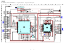
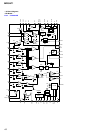
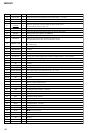
• BD BOARD IC201 CXD2664R
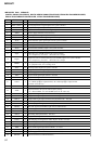
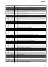
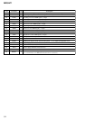
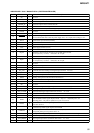
Pin No. Pin Name I/O Description
1 MNT0 (FOK) O Focus OK signal output terminal “H” is output when focus is on (“L”: NG) Not used
2 MNT1 (SHCK) O
Track jump detection signal output to the system controller
3 MNT2 (XBUSY) O
Busy monitor signal output to the system controller
4 MNT3 (SLOC) O
Spindle servo lock status monitor signal output terminal Not used
5 VDC0
— Power supply terminal (+2.5V) (for core)
6SWDTI
Writing serial data signal input from the system controller
7 SCLK I
Serial data transfer clock signal input from the system controller
8 XLAT I
Serial data latch pulse signal input from the system controller
9 VSC0
— Ground terminal (for core)
10 SRDT O
Reading serial data signal output to the system controller
11 SENS O
Internal status (SENSE) output to the system controller
12 XRST
I
Reset signal input from the system controller “L”: reset
13
SQSY O
Subcode Q sync (SCOR) output to the system controller
“L” is output every 13.3 msec Almost all, “H” is output
14
DQSY O
Digital In U-bit CD format subcode Q sync (SCOR) output to the system controller
“L” is output every 13.3 msec Almost all, “H” is output
15 RPWR I
Laser power selection signal input from the system controller
“L”: playback mode, “H”: recording mode
16 XINT O Interrupt status output to the system controller
17 TX O
Magnetic head on/off signal output to the over write head drive
18 VDIO0
— Power supply terminal (+3.3V) (for I/O)
19 OSCI I System clock signal input terminal Not used
20 OSCO I System clock signal (2048Fs=90.3168 MHz) input terminal
21 OSCN I
Control terminal for inverter and feedback resistor of internal oscillator circuit
“L”: OSCO (pin w;) is output terminal, “H”: OSCO (pin w;) is input terminal
(fixed at “H” in this set)
22 VSIO0
— Ground terminal (for I/O)
23 XTSL I
Input terminal for the system clock frequency setting
“L”: 180.6336 MHz, “H”: 90.3168 MHz (fixed at “H” in this set)
24 DIN0 I
Digital audio signal input terminal when recording mode Not used
25
DIN1 I Digital audio signal input terminal when recording mode
26
DOUT O Digital audio signal output terminal when playback mode Not used
27
DATAI I Recording data input from the USB interface
28
LRCKI I L/R sampling clock signal (44.1 kHz) input from the USB interface
29
XBCKI I Bit clock signal (2.8224 MHz) input from the USB interface
30 VDC1
— Power supply terminal (+2.5V) (for core)
31 VSC1
— Ground terminal (for core)
32
ADDT I Recording data input terminal Not used
33
DADT O Playback data output to the D/A converter
34
LRCK O L/R sampling clock signal (44.1 kHz) output to the D/A converter
35
XBCK O Bit clock signal (2.8224 MHz) output to the D/A converter
36 FS256 O
Clock signal (11.2896 MHz) output to the D/A converter
37 XWE O Write enable signal output to the D-RAM “L” active
38 XOE O Output enable signal output to the D-RAM “L” active
39 DRVDD0
— Power supply terminal (+3.3V) (for D-RAM interface)
40 DRVSS0
— Ground terminal (for D-RAM interface)
(DIGITAL SIGNAL PROCESSOR, DIGITAL SERVO SIGNAL PROCESSOR, EFM/ACIRC ENCODER/DECODER,
SHOCK PROOF MEMORY CONTROLLER, ATRAC ENCODER/DECODER)