


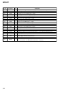
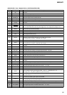
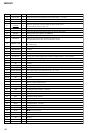
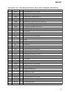
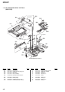
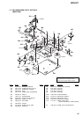

58
MDS-NT1
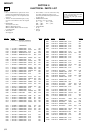
Pin No. Pin Name I/O Description
46 EXTAL I
System clock input terminal (12 MHz)
47 XTAL O
System clock output terminal (12 MHz)
48 PLLVSS
— Ground terminal (for OSC)
49 VDEC0
— Power supply terminal (+3.3V) (for CPU)
50 VSEC0
— Ground terminal (for CPU)
51 CPUCK I
Serial data transfer clock input from the system controller
52 CPUSO O
Serial data output to the system controller
53 CPUSI I
Serial data input from the system controller
54 VDEC1
— Power supply terminal (+3.3V) (for CPU)
55 VSEC1
— Ground terminal (for CPU)
56 CPUXCS I
Chip select signal input from the system controller
57 CPUINT
O Interrupt status output to the system controller
58 RESET
I Reset signal input from the system controller “L”: reset
59 VDEC2
— Power supply terminal (+3.3V) (for CPU)
60 VSEC2
— Ground terminal (for CPU)
61 VDC5
— Power supply terminal (+3.3V)
62 VSC4
— Ground terminal
63 TEST2
O Test input terminal Not used
64 TEST3
I Test input terminal Normally fixed at “L”