


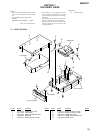

55
MDS-NT1
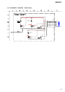
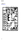
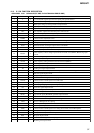
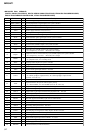
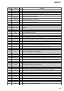
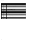
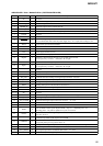
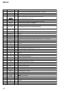
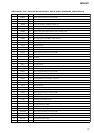
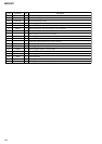
• MAIN BOARD IC301 M30835FJGP-01 (SYSTEM CONTROLLER)
Pin No. Pin Name I/O Description
1NC
— Not used
2RMCI
Remote control signal input terminal Not used
3 NETMD_SO O
Serial data output to the USB interface IC
4 NETMD_SI I
Serial data input from the USB interface IC
5 NETMD_CLK O
Serial data transfer clock output to the USB interface IC
6BYTE
I External data bus line byte selection signal input “L”: 16 bit, “H”: 8 bit (fixed at “L”)
7 CNVSS
— Not used
8, 9 NC
— Not used
10
S.RESET
I
System reset signal input terminal “L”: reset
For several hundreds msec. after the power supply rises, “L” is input, then it change to “H”
11 XOUT I
System clock input terminal (10 MHz)
12 VSS
— Ground terminal
13 XIN O
System clock output terminal (10 MHz)
14 VCC
— Power supply terminal (+3.3V)
15
NMI I Non-maskable interrupt input terminal Not used
16 DQSY
I
Digital In U-bit CD format subcode Q sync (SCOR) input terminal
“L” is input every 13.3 msec Almost all, “H” is input
17 P.DOWN
I Power down detection signal input terminal
20 SQSY
I
Subcode Q sync (SCOR) input terminal
“L” is input every 13.3 msec Almost all, “H” is input
19 to 22 NC
— Not used
23 XINT
I Interrupt status input from the mechanism deck section
24 to 26 NC
— Not used
27 I2C_CLK I/O
Communication data reading clock signal output terminal Not used
28 I2C_DATA I/O
Communication data bus input/output terminal Not used
29
SWDT
O
Writing data output to the mechanism deck section and the D/A converter
30 SRDT I
Reading data input from the mechanism deck section
31
SCLK
O
Serial data transfer clock signal output to the mechanism deck section and the D/A converter
32 RTSI
— Not used
33 to 35 NC
— Not used
36 MUTE
O Audio line muting control signal output terminal “L”: line muting on
37 ADA_RESET
O Reset signal output to the D/A converter “L”: reset
38 ADA_LATCH
O Serial data latch signal output to the D/A converter “L”: reset
39 EPM
— Not used
40, 41 NC
— Not used
42 MOD
O
Laser modulation select signal output terminal Stop: “L” Playback power: “H”
Recoding power: “H” pulse is inputted in a cycle of 2 seconds
43
LDON O
Laser diode on/off control signal output to the automatic power control circuit
“H”: laser diode on
44 CE I
Command chip enable signal output to the D-RAM
45 LIMIT-IN
I
Detection input from the sled limit-in detect switch (S101)
The optical pick-up is inner position when “L”
46 WRPWR
O Laser power select signal output terminal “L”: playback mode, “H”: recording mode
47 REC-SW I
Detection input from the recording position detect switch “L”: active
48 ADA_RESET
O Reset signal output to the mechanism deck section “L”: reset
49 SENSE I
Internal status (SENSE) signal input to the mechanism deck section