


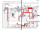

53
MDS-NT1
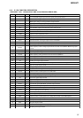
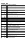
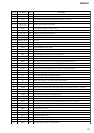
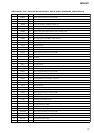
Pin No. Pin Name I/O Description
41 A11 O
Address signal output to the external D-RAM Not used
42 to 45
D0 to D3 I/O
Two-way data bus with the D-RAM
46
XCAS O Column address strobe signal output to the D-RAM “L” active
47 XRAS O Row address strobe signal output to the D-RAM “L” active
48 to 56
A00 to A02,
A05 to A10
O Address signal output to the D-RAM
57 VDC2
— Power supply terminal (+2.5V) (for core)
58 VSC2
— Ground terminal (for core)
59, 60
A03, A04 O Address signal output to the D-RAM
61 DRVDD1
— Power supply terminal (+3.3V) (for D-RAM interface)
62 DRVSS1
— Ground terminal (for D-RAM interface)
63, 64 TEST0, TEST1
I Not used
65 TEST2
O Not used
66 AVD1
— Power supply terminal (+3.3V) (analog system)
67 ASYO O Playback EFM full-swing output
68 ASYI I Playback EFM comparator slice voltage input
69 BIAS I Playback EFM comparator bias current input
70 RFI I Playback EFM RF signal input from the RF amplifier
71 AVS1
— Ground terminal (analog system)
72 PCO O Phase comparison output for master clock of the recording/playback EFM master PLL
73 FILI I Filter input for master clock of the recording/playback EFM master PLL
74 FILO O Filter output for master clock of the recording/playback EFM master PLL
75 CLTV I Internal VCO control voltage input of the recording/playback EFM master PLL
76 PEAK I Light amount signal (RF/ABCD) peak hold input from the RF amplifier
77 BOTM I Light amount signal (RF/ABCD) bottom hold input from the RF amplifier
78 ABCD I Light amount signal (ABCD) input from the RF amplifier
79 FE I Focus error signal input from the RF amplifier
80 AUX1 I Auxiliary signal (I
3 signal/temperature signal) input from the RF amplifier
81 VC I Middle point voltage (+1.65V) input from the RF amplifier
82 ADIO O Output terminal for the test
83 ADRT I A/D converter operational range upper limit voltage input terminal (fixed at “H” in this set)
84 ADRB I A/D converter operational range lower limit voltage input terminal (fixed at “L” in this set)
85 SE I Sled error signal input from the RF amplifier
86 TE I Tracking error signal input from the RF amplifier
87 AVD2
— Power supply terminal (+3.3V) (analog system)
88 AVS2
— Ground terminal (analog system)
89 DCHG I Connected to the +3.3V power supply
90 APC I Error signal input terminal for laser digital automatic power control Not used
91 ADFG
I
ADIP duplex FM signal (22.05 kHz ± 1 kHz) input from the RF amplifier
92 VDIO1
— Power supply terminal (+3.3V) (for I/O)
93 VSIO1
— Ground terminal (for I/O)
94 F0CN O Filter f0 control signal output to the RF amplifier
95 VDC3
— Power supply terminal (+2.5V) (for core)
96 VSC3
— Ground terminal (for core)
97 XLRF O Serial data latch pulse signal output to the RF amplifier
98 CKRF O Serial data transfer clock signal output to the RF amplifier
99 DTRF O Writing serial data output to the RF amplifier