


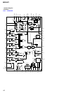

56
MDS-NT1
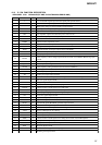
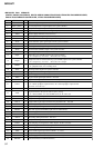
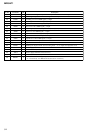
Pin No. Pin Name I/O Description
50 PLAY-SW I
Detection input from the playback position detect switch “L”: active
51 XLATCH
O Serial data latch pulse signal output to the mechanism deck section
52 SCL O
Serial clock signal output to the EEPROM
53 OUT-SW I
Detection signal input from the loading-out detect switch (S103)
“L” at a load-out position, others: “H”
54 XBUSY I
Busy monitor signal input from the mechanism deck section
55 SHOCK I
Track jump detection signal input from the mechanism deck section
56 EEP-WP O
Writing protect signal output to the EEPROM
57 SDA I/O
Two-way data bus with the EEPROM
58 REFLECT I
Detection input from the disc reflection rate detect switch
“L”: high reflection rate disc, “H”: low reflection rate disc
59 PROTECT SW I
REC-proof claw detection signal input from the protect detect switch
“H”: write protect
60 VCC
— Power supply terminal (+3.3V)
61 EEPNET-WP
— Not used
62 VSS
— Ground terminal
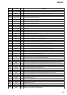
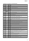
63 LD-LOW
O Loading motor drive voltage control signal output terminal “H” active
64 LOAD OUT O
Loading motor control signal (load-in direction) output terminal “H” at a load-in
65 LOAD OUT O
Loading motor control signal (eject direction) output terminal “H” at a eject
66 to 69 TEST
I Test input terminal Not used
70 to 72 NC
— Not used
73 NETMD_INT
I Interrupt status input from the USB interface IC
74 NETMD_XCS O
Chip select signal output to the USB interface IC
75 NETMD_RESET
O Reset signal output to the USB interface IC “L”: reset
76 NETMD_PLLSW
O PLL function on/off control signal output to the USB interface IC “L”: PLL on
77 NETMD_VBUS I
USB connect detection signal input terminal “H”: USB on
78, 79 NC
— Not used
80 LED4 O
LED drive signal output terminal Not used
81, 82 LED3, 2 O
LED drive signal output terminal
83 FLCS
— Not used
84 LED1 O
LED drive signal output terminal
85
JOG0 I Jog dial pulse input terminal Not used
86
JOG1 I Jog dial pulse input terminal Not used
87 IOP
— Not used
88
SEL1 I Destination setting terminal
89
SEL0 I Model setting terminal
90, 91 NC
— Not used
92 KEY2 I
key input terminal Not used
93 KEY1 I
B/> key input terminal
94 AVSS
— Ground terminal
95 KEY0 I
x/Z key input terminal
96
VREF I Reference voltage (+3.3V) input terminal
97 AVCC
— Power supply terminal (+3.3V)
98 NC
— Not used
99 FLDT
— Not used
100 FLCK
— Not used