


User Connections 29
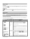
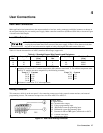
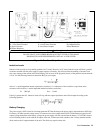
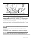
Output Safety Cover ô Analog Connector í– Output Bus Bar
÷ – Local Sense Terminal û + Local Sense Terminal ø+ Output Bus Bar
ù Signal Common î Local Sense Jumpers ü Rear Knockouts
ê Bottom Knockout
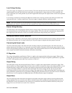
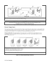
Insert screwdriver blade in slot and pry out Bend along joint and break off
WARNING
DO NOT LEAVE UNCOVERED HOLES IN OUTPUT COVER. IF TOO MANY
KNOCKOUTS HAVE BEEN REMOVED, INSTALL A NEW COVER.
Figure 4-3. Rear Panel Output Connections
Inductive Loads
Inductive loads provide no loop stability problems in CV mode. However, in CC mode inductive loads will form a parallel
resonance network with the power supply's output capacitor. Generally, this will not affect the stability of the unit, but it
may cause ringing of the current in the load. Ringing will not occur if the Q (quality factor) of the parallel resonant network
is
≤
1.0. Use the following formula to determine the Q of your output.
Q=
L1
RCxtint eR+
where: C = model-dependent internal capacitance (see below); L = inductance of the load; Rext = equivalent series
resistance of the load; R
int
= model-dependent internal resistance (see below):
C=
7,000
µ
F
R
int
=
14 m
Ω
If the Q is greater than 0.5, inductive loads will ring with the output capacitance and will be damped according to the
following equation:
Battery Charging
The power supply's OVP circuit has a downprogrammer FET that discharges the power supply output whenever OVP trips.
If a battery (or other external voltage source) is connected across the output and the OVP is inadvertently triggered or the
output is programmed below the battery voltage, the power supply will sink current from the battery. To avoid this, insert a
reverse blocking diode in series with the ⊕ output of the unit. Connect the diode cathode to the + battery terminal and the
diode anode to the ⊕ output terminal of the unit. The diode may require a heat sink.