


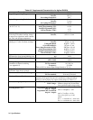
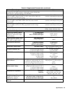
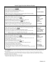

Specifications 95
Table A-2. Supplemental Characteristics (continued)
Parameter Value
Command Processing Time
(Average time for output voltage to change after receipt of digital data
when the unit is connected directly to the GPIB Bus):
20 ms
Output Voltage Rise Time/Fall Time
(time for output to change from 90 % to 10% or from 10% to 90% of its
total excursion with full resistive load)
100 ms/200 ms
(excludes command processing time)
Full-load Programming Speed Up Time/Down Time
(time for output to settle within 4 LSBs of the final value with full
resistive load)
200 ms/475 ms
(excludes command processing time)
No-load Programming Discharge Time
(time for output to fall to 0.5V when programmed from full voltage
to zero volts)
650 ms
(excludes command processing time)
Monotonicity:
Output is monotonic over entire rated
voltage, current, and temp. range.
Auto-Parallel Configuration: Up to 3 units
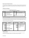
Analog Programming (IP&VP)
(signal source must be isolated;
VP input is referenced to output
signal common)
VP Input Signal:
VP Input Impedance:
IP to –IP Differential Input:
0 to –4.15 V
60 k
Ω
, nominal
0 to +6.75 V
Current Monitor Output (+IM)
(signal range corresponds to from
0% to 100% of output current)
IM Output Signal:
Output Impedance:
–0.25 to –8.08 V
490
Ω
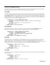
Nonvolatile Savable States Memory Locations:
Memory Write Cycles:
Factory Prestored State:
5 ( 0 through 4)
40,000, typical
Location 0
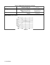
Digital Port Characteristics Maximum ratings: 16.5 Vdc between terminals 1 & 2;
3&4; and from 1 or 2 to chassis.
FLT/INH Terminals 1 & 2
I
ol
(low-level output current)
V
ol
(low-level output voltage)
1.25 mA maximum
0.5 V maximum
FLT/INH Terminals 3 & 4
V
il
(low-level input voltage)
V
ih
(high-level input voltage)
I
il
(low-level input current)
tw (pulse width)
td (time delay)
0.8 V maximum
2.0 V minimum
1 mA
100
µ
s, minimum
4 ms, typical
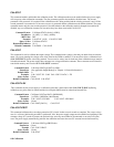
Digital OUT Port 0,1,2 -
Open Collector:
I
oh
(high-level output leakage @ 16.5V)
I
oh
(high-level output leakage @ 5.25V)
I
ol
(low-level output sink current @ 0.5V)
I
ol
(low-level output sink current @ lV)
100
µ
A (ports 0,1); 12.5 mA (port 2)
100
µ
A (ports 0,1); 250
µ
A (port 2)
4 mA
250 mA
Digital IN Port 2 -
Internal 4.64 k Pullup:
I
il
(low-level input current @ 0.4 V)
I
ih
(high-level input current @ 5.25 V)
V
il
(low-level input voltage)
V
ih
(high-level input voltage)
1.25 mA
250
µ
A
0.8 V maximum
2.0 V minimum
GPIB Interface Capabilities Languages:
Interface:
SCPI (default); Compatibility
AH1, C0, DC1, DT1, E1, LE4,
PP0, RL1, SH1, SR1, TE6
Serial Link Capabilities
(multiple units sharing one
GPIB primary address)
Maximum number of units:
Maximum number of linked units:
Maximum total chain cable length:
16
15
30 m (100 ft)
Recommended Calibration
Interval:
1 year