


41
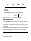
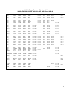
+5V and PCLR Circuits:
Node Measurement
U1-8
≈ 3.5Vdc
U1-2 = 4 Vdc
U1-3 = 4.2Vdc
U1-4 = 4.2Vdc
U1-6
≈50mVdc
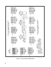
Clock Signals (see clock waveforms in Figure 3-3)
Node Measurement Source
C7+,C8+ = 12MHz (see waveform) Y2
J5-8 = 6MHz (see waveform) U14
U35-12
≈ 50mVdc (see waveform)
U35
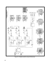
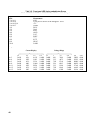
Data Lines Check that all data and address lines are toggling. Address and data lines go to the following IC's:
Address Lines Data Lines
U6: A0 to A15 U6: D0 to D7
U8: A0 to A15 U8: D0 to D7
U12: A0 to A4 U12: D0 to D7
U14: A8 to A15 U14: D0 to D7
U16: A0 to A7 U16: D0 to D7
U17: A0 to A2 U17: D0 to D7
U36: A7 to A15
Note: Data and address lines may not toggle if one line is shorted either high or low. If no short is found, replace
all socketed IC's. If the data lines still do not toggle, replace the GPIB (A8) assembly.
Node Measurement
A0 to A15 Toggling
D0 to D7 Toggling
Secondary Interface Troubleshooting
Secondary interface troubleshooting checks the operation of the voltage, current, and readback DACs as well as analog
multiplexer and secondary microprocessor. The analog multiplexer is checked in the Readback DAC troubleshooting
procedure. The secondary microprocessor can only be checked using secondary SA (refer to Signature Analysis).
Voltage and Current DAC
The voltage and current DACs can be checked either from the front panel or by secondary SA. Refer to Signature Analysis
to troubleshoot the voltage and current DACs in this manner.
Note: To troubleshoot the voltage and current DACs from the front panel if the unit has failed selftest, place
jumper A8J5 in the skip selftest position (see Table 3-2). This lets you operate the unit even though it fails
the internal selftest.