


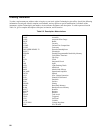

75
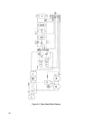
Control Voltage Comparator.
This circuit compares the voltage at the CONTROL PORT (represents power required at
output) with PRIMARY CURRENT RAMP voltage (represents energy being stored for transfer to output). When RAMP
voltage exceeds CONTROL PORT voltage, the Control Voltage Comparator generates the
CONTROL LIMIT signal to
turn the PWM off. The CONTROL PORT is biased to approximately + 1.3 volts. Whichever control signal, CC or CV, is
more negative (calling for less output power) forward biases its output diode and determines the voltage at the CONTROL
PORT.
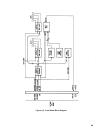
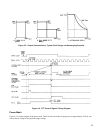
As can be seen from the waveforms in Figure 4-4, there is a delay between the time when PRIMARY CURRENT RAMP
voltage exceeds the CONTROL PORT voltage and the time when the FETs turn off. This delay consists of the comparator
switching time, gate delays, transformer delay, and FET turn-off time, and it results in a certain amount of power being
transferred to the output after the desired off time. If the CONTROL PORT voltage is at a very low level (unit supplying
little or no output power), this power may exceed the amount required by the load. To eliminate the delay, the Control
Voltage Comparator includes an initial ramp circuit that generates a small ramp voltage before the FETs are turned on. The
added ramp voltage starts with the 20KHz clock pulse, and causes the combined-ramp voltage to exceed the CONTROL
PORT voltage earlier, thereby effectively eliminating the FET turn-off delay.
Status Drivers. Inputs from the CC and CV Circuits indicate which circuit, if either, is regulating the power supply output.
If neither circuit is regulating the output (load calling for more power than the power supply can deliver), logic circuits
within Status Driver block determine that output is unregulated.
In GPIB units, CC and CV signals go to the microcomputer, which will take appropriate action, including lighting
front-panel indicators. In non-- GPIB units, Status Driver outputs go to front-panel indicators.
20KHz Clock. This circuit contains a 320KHz crystal oscillator and dividers that produce 40KHz, 20KHz, and 1.25KHz
signals. Both the 320KHz and 20KHz signals are supplied to the PWM, with the 20KHz signal controlling the repetition
rate of the PWM.
The 40 KHz signal is supplied to the +5V Bias Supply Circuit to synchronize the PWM in that circuit to the main power
supply PWM. The 1.25KHz output is supplied to the Time Delay Circuit for generating the time delay used to control the
power supply turn-on sequence.
The 1.25KHz signal is subsequently disabled by the AC FAULT output from the Time Delay Circuit at the end of the time
delay.
Pulse Width Modulator (PWM). The PWM generates the ON and OFF pulses that control the power FETs in the power
mesh. ON pulses are generated at a 20KHz rate, and, as can be seen in Figure 4-4, are initiated by the first 320KHz dock
pulse after the start of the 20KHz clock pulse. When the FET switches turn on, current flows through the Primary Current
Monitor transformer on the main board, and the Primary CURRENT RAMP voltage starts to rise. OFF pulses are normally
initiated when CONTROL LIMIT becomes active (low), indicating that the ramp voltage has exceeded the CONTROL
PORT voltage. However, an off pulse can be initiated by any one of a number of other signals.
An overtemperature (
OT ), overvoltage ( OV ), remote inhibit, AC FAULT condition or an INHIBIT signal from GPIB
will initiate an OFF pulse, and will also trigger the Down Programmer to reduce output voltage to zero. These conditions
will also cause
PWM OFF to be sent to the TurnOn Overshoot Control Circuit.
OFF pulses can also be initiated by
POWER LIMIT and by the trailing edge of the 20KHz clock signal. The 20KHz clock
signal ensures that even if nothing else, such as CONTROL LIMIT or POWER LIMIT , initiates an OFF pulse, the FET
duty cycle will be limited to less than 50%.
Overvoltage Protection (OVP). The OVP circuit monitors the power supply output voltage and compares it to a preset
limit determined by a front-panel OVP ADJUST potentiometer. If the output voltage exceeds the limit, the OVP Circuit
initiates a PWM OFF pulse, which also triggers the Down Programmer. The OVP Circuit lathes itself until it receives OV
CLEAR or ac power is turned off.