


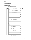
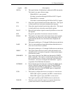
5.2 Logical Interface
C141-E050-02EN 5-7
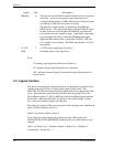
5.2.1 I/O registers
Communication between the host system and the device is done through input-
output (I/O) registers of the device.
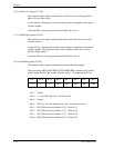
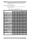
These I/O registers can be selected by the coded signals, CS0-, CS1-, and DA0 to
DA2 from the host system. Table 5.2. shows the coding address and the function
of I/O registers.
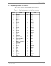
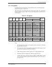
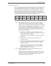
Table 5.2 I/O registers
I/O registers
Read operation
Write operation
Command block registers
L
H
L
L
L
Data
Data
X’1F0’
L
H
L
L
H
Error Register
Features
X’1F1’
L
H
L
H
L
Sector Count
Sector Count
X’1F2’
L
H
L
H
H
Sector Number
Sector Number
X’1F3’
L
H
H
L
L
Cylinder Low
Cylinder Low
X’1F4’
L
H
H
L
H
Cylinder High
Cylinder High
X’1F5’
L
H
H
H
L
Device/Head
Device/Head
X’1F6’
L
H
H
H
H
Status
Command
X’1F7’
L
L
X
X
X
(Invalid)
(Invalid)
—
Control block registers
H
L
H
H
L
Alternate Status
Device Control
X’3F6’
H
L
H
H
H
— —
X’3F7’
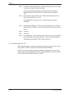
Notes:
1. The Data register for read or write operation can be accessed by 16 bit data
bus (DATA0 to DATA15).
2. The registers for read or write operation other than the Data registers can be
accessed by 8 bit data bus (DATA0 to DATA7).
3. When reading the Drive Address register, bit 7 is high-impedance state.
4. H indicates signal level High and L indicates signal level Low.
And the LBA mode is specified, the Device/Head, Cylinder High, Cylinder
Low, and Sector Number registers indicate LBA bits 27 to 24, 23 to 16, 15
to 8, and 7 to 0.
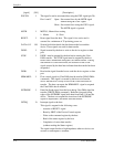
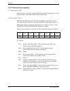
Host I/O
address
DA0DA1DA2CS1
–
CS0
–