


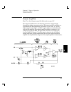
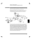
Waveform DAC/Amplitude Leveling/Waveform RAM
Block 4 on block diagram page 129; Schematic on page 134.
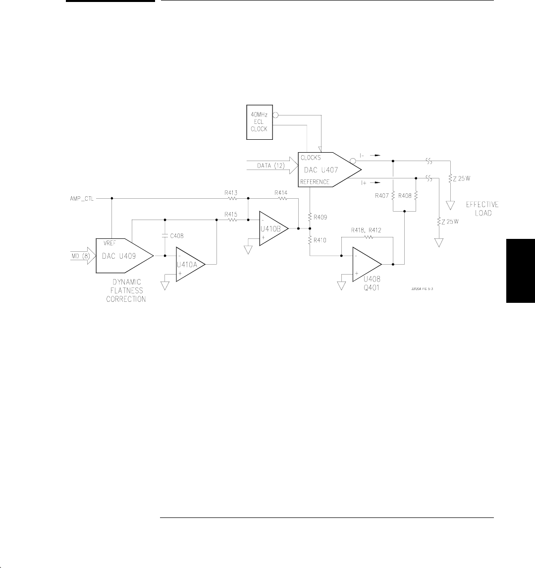
The Waveform DAC, U407, converts 12-bit digital data from waveform
RAM’s U404 and U405 into positive and negative analog voltages.
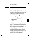
A simplified diagram of the Waveform DAC circuitry is shown below.
The preattenuator, filters, and associated circuits in the output signal path
provide an approximate 25
W load for the Waveform DAC. The Waveform
DAC nominally produces a 40 mA differential output current — yielding
differential 1 Vac output signals. Wave shape (amplitude) data is loaded
into the waveform RAM by the main controller CPU U102. Once loaded,
these data are addressed by the DDS ASIC. The rate at which addresses
are incremented determines the output waveform frequency. Waveform
RAM output data is latched and shifted to ECL levels by U402 and U403
for input to the waveform digital-to-analog converter (DAC) U407. DDS
ASIC U206, waveform data latches U402 and U403, and the Waveform
DAC U407 are clocked at 40 MHz. The 40 MHz clock is generated by
oscillator U413 and ECL level-shifter U401.
5
Chapter 5 Theory of Operation
Waveform DAC/Amplitude Leveling/Waveform RAM
93