


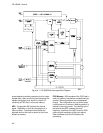
Triggering. There are two main trigger circuits
that trigger four trigger sources. The two trigger
circuits are the analog trigger and the logic trigger.
The analog trigger IC operates as a multichannel
Schmidt trigger/comparator. A trigger signal (a
copy of the analog input signal) from each of the
inputs is directed to the analog trigger IC inputs.
The trigger signal is continuously compared with
the trigger reference level selected by the user.
Once the trigger condition is met, the trigger TRUE
signal is fed to the logic trigger, which begins the
acquisition and store functions by way of the time
base.
The four trigger sources are Channel 1, Channel 2,
Intermodule Bus (IMB), and external BNC. The
operation of the input channels was discussed
previously. The IMB trigger signal is sent directly
to the logic trigger. External triggering is provided
by the BNC input of the 16500A Logic Analysis
System mainframe.
Time Base. The time base provides the sample
clocks and timing necessary for data acquisition.
It consists of the 100 MHz reference oscillator and
time base hybrid.
The 100 MHz reference oscillator provides the
base sample frequency.
The time base hybrid has programmable dividers
to provide the rest of the sample frequencies
appropriate for the time range selected. The time
base uses the time-stretched output of the fine
interpolator to time-reference the sampling to the
trigger point. The time base has counters to
control how much data is taken before (pre-trigger
data) and after (post-trigger data) the trigger event.
After the desired number of pre-trigger samples
has occurred, the Time base hybrid sends a signal
to the Logic Trigger (trigger arm) indicating it is
ready for the trigger event. When the trigger
condition is satisfied, the Logic Trigger sends a
signal back to the time base hybrid. The time base
hybrid then starts the post-trigger delay counter.
When the countdown reaches zero, the sample
clocks are stopped and the CPU is signaled that
the acquisition is complete. The Fine Interpolator
is a dual-slope integrator that acts as a
time-interval stretcher. When the logic trigger
receives a signal that meets the programmed
triggering requirements, it signals the time base.
The time base then sends a pulse to the fine
interpolator. The pulse is equal in width to the time
between the trigger and the next sample clock.
The fine interpolator stretches this time by a factor
of approximately 500. Meanwhile, the time base
hybrid runs a counter with a clock derived from the
sample rate oscillator. When the interpolator
indicates the stretch is complete, the counter is
stopped. The count represents, with much higher
accuracy, the time between the trigger and the first
sample clock. The count is stored and used to
place the recently acquired data in relationship
with previous data.
AC Cal. The AC Cal is a multiplexer circuit that
can provide several signals to the Probe
Compensation/AC Calibrator output on the rear
panel. The signal provided depends on the mode
of the instrument. It can be either a probe
compensation signal, a pulse representing the
trigger event, signals used for self-calibration, or
the 100 MHz reference oscillator when sample
period is 1 ns.
DC Cal. The DC Cal output, a rear panel signal, is
used for self-calibration. It is one output from the
16-channel DAC.
Digital Interface. The Digital Interface provides
control and interface between the system control
and digital functions in the acquisition circuitry.
Analog Interface. The Analog Interface provides
control of analog functions in the acquisition
circuitry. It is primarily a 16-channel DAC with an
accurate reference and filters on the outputs. It
controls channel offsets and trigger levels, and
provides the DC Cal output.
HP 16532A - Service
6-3