


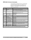


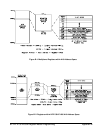
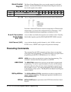

Register Offset The register offset is the register’s location in the block of 64 address bytes.
For example, with a LADDR of 112 the multiplexer’s Scan Channel Delay
Register has an offset of 08
16
. When you write a command to this register,
the offset is added to the base address to form the register address:
DC0016 + 0816 = DC08
16
(A16 outside the command module)
1FDC00
16
+ 08
16
= 1FDC08
16
(A16 inside the command module)
or
56,320 + 8 = 56,328 (A16 outside the command module)
2,087,936 + 8 = 2,087,944 (A16 inside the command module)
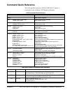
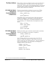
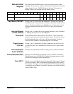
Register Descriptions
There are six WRITE and two READ-only registers on the multiplexer.
You can READ-back three of the WRITE registers. This section contains a
description and a bit map of each register. Note that the bit names with an *
after them are True (asserted) when low (zero). An X represents a "do not
care" situation and a 1 always represents 1.
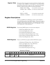
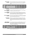
WRITE Registers The following WRITE registers are located on the multiplexer:
• Status/Control Register (base + 04
16
)
• Scan Control Register (base + 06
16
)
• Scan Channel Delay Register (base + 08
16
)
• Scan Channel Configuration Register (base + 0A
16
)
• Direct Channel Configuration Register (base + 0C
16
)
• Direct Control Register (base + 0E
16
)
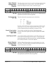
READ Registers There are two READ-only registers and three READ-back registers.
• Manufacturer ID Register (base + 00
16
) READ-only
• Device Type Register (base + 02
16
) READ-only
• Status/Control Register (base + 04
16
)
• Scan Control Register (base + 06
16
)
• Scan Channel Delay Register (base + 08
16
)
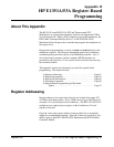
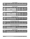
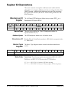
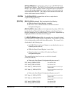
Manufacturer ID Register
base + 00
16
1514131211109876543210
Write Undefined
Read Device
Class
Address
Space
Manufacturer ID
84 HP E1351A/53A Register-Based Programming Appendix B