


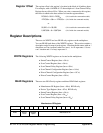
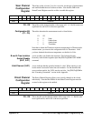
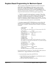

Scan Control
Register
The Scan Control Register allows you to clear the scan list, set the trigger
mode and reset the pointer to the beginning of the scan list. This register is
a READ-back register, allowing you to verify the state of the WRITE
register.
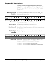
base + 06
16
1514131211109876543210
Write Undefined X X X RST
PTR
CNT
EN
IMM
EN
DBS
EN
CLR
SCN
Read Undefined 1 1 1 1 CNT
EN
IMM
EN
DBS
EN
CLR
SCN
Clear Scan List
(CLR SCN)
Writing a one (1) in this bit clears the scan list. The bit must be set back to
zero (0) after flushing. CLR SCN (Read) returns the state of the bit.
Digital Bus Enable
(DBS EN)
Writing a one (1) enables the digital bus trigger mode. A zero (0) disables
it. DBS EN (Read) returns the state of the bit.
Immediate Enable
(IMM EN)
Writing a one (1) in this bit sets trigger to immediate, which means that as
soon as the first channel is closed by the TRG INT, the entire scan list is run
without any further triggering. Channel advance speed is determined by the
delay time specified. This has extremely limited applications.
Continuous Enable
(CNT EN)
Writing a one (1) in this bit enables the card to continually cycle through the
scan list. When this bit is enabled, the last channel in a scan list resets the
pointer back to the beginning of the scan list.
Reset Pointer
(RST PTR)
Writing a one (1) resets the pointer back to the beginning of the scan list.
CNT EN true automatically resets pointer at end of scan list. If CNT EN is
set true, an interrupt also resets the pointer. If CNT EN is set false, the last
channel in the scan list generates an interrupt if the channel is valid (VLD*
set true).
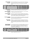
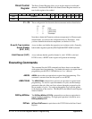
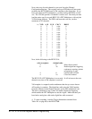
Scan Channel
Delay Register
The Scan Channel Delay Register sets the SETTling:TIME, the time between
receipt of a channel closing trigger and the Channel Closed pulse. The
delay is 2
n
µS and
n
has a range of 0 to 15. D3 to D0 set
n
, and D0 is the
least significant bit. This register is a read-back register, allowing you to
verify the state of the WRITE register.
base + 08
16
1514131211109876543210
Write Undefined XXXXD3D2D1D0
Read Undefined 1 1 1 1 D3 D2 D1 D0
D3 - D0 D0 is the least significant bit, D3 is the most significant. These bits
designate a number between 0 and 15 for
n
.
88 HP E1351A/53A Register-Based Programming Appendix B