


Theory of Operation
4–2
VITS100 NTSC VITS Inserter Instruction Manual
The power inductor is driven by switching the voltage to its primary winding on
and off at a rate of approximately 45 kHz. The power inductor is used as an
energy storage device. Energy is stored in the primary during the first half of the
switching cycle. On the second half of the switching cycle, the stored energy is
transferred to the secondaries.
Regulation is accomplished through feedback from the +5 V supply to the Pulse
Width Modulator that controls the primary voltage. The Pulse Width Modulator
varies the length of time that voltage is applied to the primary changing the
amount of stored energy.
All primary voltages are referenced to a floating ground, not chassis ground. An
isolation transformer or a differential amplifier is therefore required for trouble-
shooting the circuitry in the primary and the Pulse Width Modulator.
Circuit Description
The following circuit description takes you down to the component level.
Because of the arrangement of circuits on the schematic diagrams, most of the
functional headings cover circuits that appear on more than one schematic
diagram.
In this discussion active-low signals are denoted by overbars (like this
). Signal
names are in lower case and enclosed in quotation marks (“like this”).
The circuitry that generates the test signals for insertion appears on three of the
schematic diagrams located in the Diagrams section of this manual. Key
circuitry is located on diagrams 1 (Test Signal Memory), 3 (H & V Counters,
Source Identification & Bypass Controls), and 7 (Analog Output).
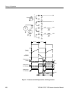
Diagram 3. Test signal generation starts with a 4
FSC
clock that clocks the
Horizontal Counter, U28, to provide 910 counts per line of video. In addition,
this counter decodes the backporch clamp pulse, for the test signal. The output of
the Horizontal Counter drives a Horizontal Decoder PROM, U27, to provide
timing signals for various functions. The Horizontal Counter is reset by the
frame pulse, from the genlock circuitry in order to time the test signals to
program video.
A once-per-line pulse from the Horizontal Decoder PROM (pin 14) enables the
Vertical Counter, U24. This synchronous output of the Vertical Counter drives
the Vertical Decoder PROM, U25. Output of U25 is latched twice per line by
U26, which is clocked by the “vlatch” from U27 (pin 16).
Diagram 1. Test signal data is stored in PROMs U4, U5, and U6. U4 and U5 store
the eight MSBs of alternate data samples. U6 stores the four LSBs for all data
Test Signal Generation