


Theory of Operation
4–10
VITS100 NTSC VITS Inserter Instruction Manual
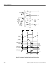
These requirements are met by using a FET, Q17, in the emitter circuit to turn
Q16 on and off. The modulated pulse from U78 gates Q17.
When Q17 turns on, base current flows in Q16 through R149 and CR22 (which
turns on) and current flows in the primary winding of T1, completing the circuit
through Q16, Q17, and R163 into the floating ground. CR20 keeps Q16 from
going into hard saturation by diverting some of the base current into the collector
when it turns completely on.
When Q17 turns off, the current path from the collector of Q16 to its emitter no
longer exists. For a brief time, the collector current becomes reverse flowing
base current in Q16. When this current flows out of the base through CR21, it
charges the housekeeping capacitor, C113, which turns Q16 off very rapidly.
When Q16 turns off, a voltage spike appears at its collector. A combination of
reflected secondary voltages, input voltage, and transformer leakage inductance
produces a voltage spike of high magnitude. A snubber circuit consisting of
R153, CR19, and C97 dissipates some of the energy in the T1 leakage
inductance.
12 V is generated from the 15 V secondary output of T1. The 15 V at C102 and
C103 passes through RC filters and is applied to the three-terminal linear
regulators (U73 and U85) to derive the + and –12 V outputs.
Over-voltage protection is provided on the +5 V output by a crowbar circuit
composed of Q15, VR4, and R146. If the +5 V output exceeds approximately
+5.5 V, VR4 will start to conduct. When VR4 draws enough current through
R146 to raise the gate voltage for Q15 (an SCR) above its cathode by approxi-
mately 0.7 V, VR4 turns on and shorts the +5 V output to ground, forcing the
primary circuit into current limit.
Diagram 9. The regulated 5 V supplies used by the ADC and the DAC are
generated from the 12 V supplies by three-terminal linear regulators (U52 and
U53).