


Theory of Operation
VITS100 NTSC VITS Inserter Instruction Manual
4–5
The circuitry that controls signal switching appears on three of the schematic
diagrams in the Diagrams section of this manual. Key circuitry is located on
diagrams 1 (Test Signal Memory), 2 (Test Signal Select), and 5 (Program Input,
Sync Stripper, VIRS Detection, & Genlock A/D Input).
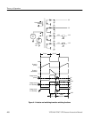
Diagram 2. Signal selection is accomplished with four dual in-line package (DIP)
switches, S1, S2, S3, and S4. The lines from the switches are multiplexed by
U18, U19, U20, and U21
to select the appropriate switch segments at the correct time (S1 segments 1
through 4 during line 17 odd fields, for example).
The multiplexing is controlled by two bits from the Vertical Decoder and the
field signal from the Vertical Counters on diagram 3. Two PALs, U16 and U17,
located on diagram 1, decode control signals and latch the signal selections. U16
latches the bits to the test signal PROMs, and decodes when the source ID signal
is requested. Signals “vdrive” and “vsync” force the generation of vertical sync.
Diagram 5. U17, on diagram 1, decodes when Auto VIRS has been requested. It
enables the circuitry that compares program video to the VIRS test signal to
determine if VIRS is present on program video. U46 is an operational amplifier
that subtracts low-pass filtered program video from filtered test signals and
drives U47A and U47B, a window comparator.
If the program signal and the test signal match closely enough, the comparator
output remains high and the output of an OR gate, U48A, remains high; a one
shot, U71B, is not triggered. The OR gate can only trigger the one shot when
U17, on diagram 1, determines that Auto VIRS has been requested and drives
“virsamp
” low. The signal “virpres” from U71B returns to U17, on diagram 1,
and “ccvirs” from U17 is sent to U14 to control insertion.
Diagram 1. U17 also decodes “dvdrive” and “dvsync” which are delayed from
“vdrive” and “vsync” by a half line and therefore are timed with the actual test
signals that are generated.
U14 takes the information from U16 and U17, “chswt” (the insertion timing
signal), and other timing signals; it then determines two control signals for the
program channel switch, “sw0” and “sw1,” and one signal to choose between
source ID generation and test signal generation, “ts/char
.”
The circuitry that controls source ID generation appears on two of the schematic
diagrams in the Diagrams section of this manual. Key circuitry is located on
diagrams 1 (Test Signal Memory) and 3 (H & V Counters, Source Identification
& Bypass Controls).
Signal and Switching
Control
Source ID Generation