


Emerson Process Management GmbH & Co. OHG A-25
A
Appendix
X-STREAM XEFD
Instruction Manual
HASXEDE-IM-EX
03/2012
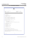
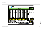
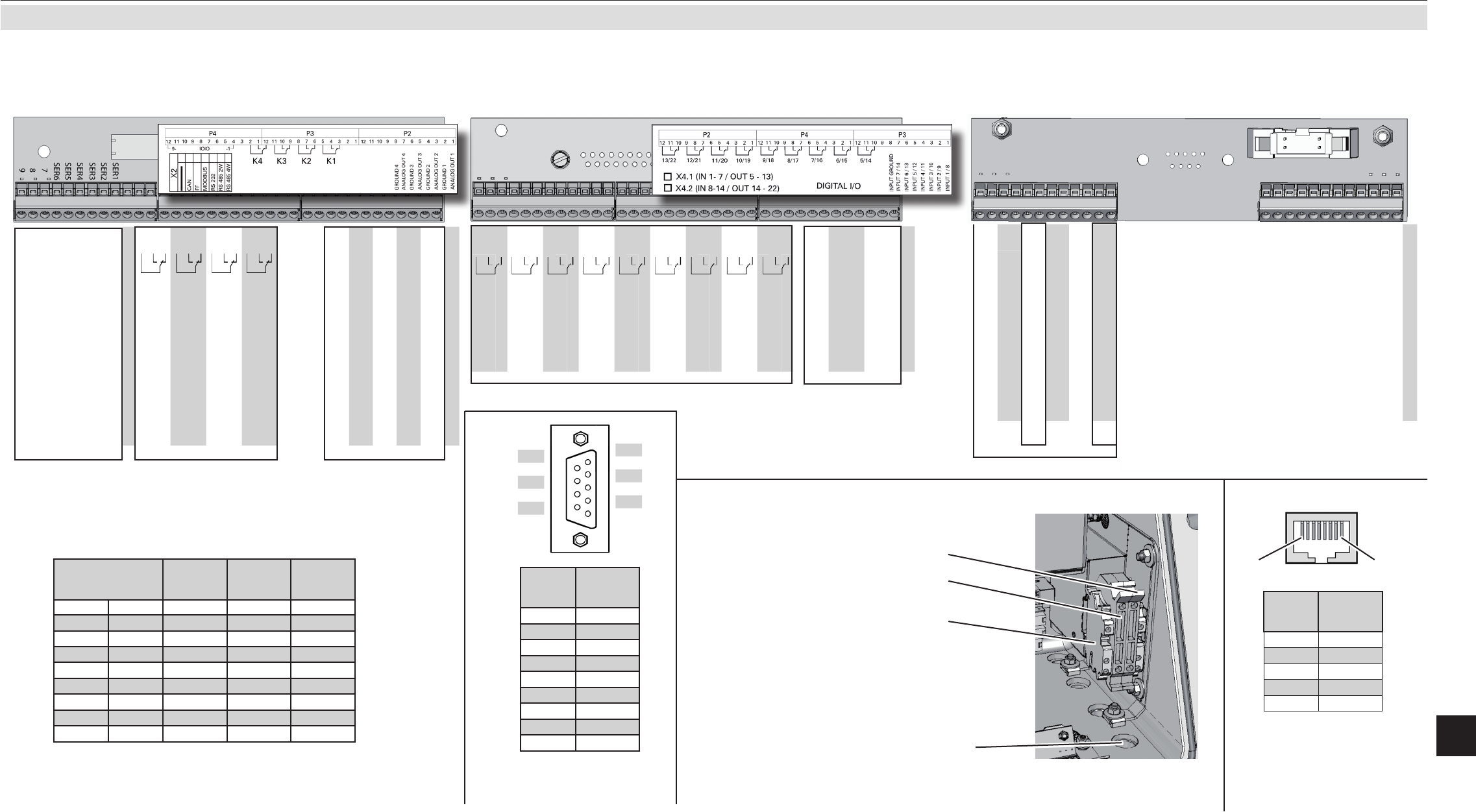
A.5 Assignment of Terminals and Socket
A.5 Assignment of Terminals and Sockets
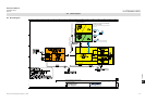
Power terminals
Flameproof housing
L
PE
N
Power cord
entry
L= Line
N= Neutral
PE= Protective Earth
Service Port Connector -
Serial RS 232 interface
Ethernet connector
for Modbus
Pin 1 Pin 8
Pin no.
Signal
1 TX+
2 TX-
3 RX+
6 RX-
other not used
Note!
Line and neutral terminals with
built-in fuse holders
XSTA: Standard strip with standard and optional signals
XSTD: Optional strips with
7 Dig Inputs and 9 Dig Outputs each
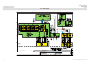
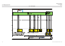
Pin
9
8
7
6
Pin
5
4
3
2
1
Pin no.
RS 232
1 Common
2 RXD
3 TXD
4 not used
5 Common
6 not used
7 not used
8 not used
9 not used
*)
See table below
**)
Conguration of relay output termi-
nals as per standard factory setting
(NAMUR status signals)
XSTI: Analog inputs
Analog Inputs
Pin Signal
P3.1 not used
P3.2 not used
P3.3 not used
P3.4 not used
P3.5 not used
P3.6 not used
P3.7 not used
P3.8 not used
P3.9 not used
P3.10 not used
P3.11 not used
P3.12 not used
P2.1 BR 1 t a wire bridge here to apply analog
P2.2 BR 1 signal in current mode to input 1
P2.3 Input 1 high (+)
P2.4 Input 1 high (+)
P2.5 Input 1 low (-)
P2.6 Input 1 low (-)
P2.7 BR 2 t a wire bridge here to apply analog
P2.8 BR 2 signal in current mode to input 2
P2.9 Input 2 high (+)
P2.10 Input 2 high (+)
P2.11 Input 2 low (-)
P2.12 Input 2 low (-)
{
}
{
}
IN1
Mode
IN2
Mode
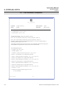
Pin Signal
P2.1 Channel 1, (+) 4 (0) - 20 mA
P2.2 Channel 1, GND
P2.3 Channel 2, (+) 4 (0) - 20 mA
P2.4 Channel 2, GND
P2.5 Channel 3, (+) 4 (0) - 20 mA
P2.6 Channel 3, GND
P2.7 Channel 4, (+) 4 (0) - 20 mA
P2.8 Channel 4, GND
P2.9 Channel 5, (+) 4 (0) - 20 mA
P2.10 Channel 5, GND
P2.11 not used
P2.12 not used
P3.1 not used
P3.2 not used
P3.3 Output 1 (Failure), NC
P3.4 Output 1 (Failure), NO
P3.5 Output 1 (Failure), COM
P3.6 Output 2 (Maintenance Request), NC
P3.7 Output 2 (Maintenance Request), NO
P3.8 Output 2 (Maintenance Request), COM
P3.9 Output 3 (Out of Spec), NC
P3.10 Output 3 (Out of Spec), NO
P3.11 Output 3 (Out of Spec), COM
P3.12 Output 4 (Function check), NC
P4.1 Output 4 (Function check), NO
P4.2 Output 4 (Function check), COM
P4.3 not used
P4.4
P4.5
P4.6
P4.7
P4.8
P4.9
P4.10
P4.11
P4.12
Relay Outputs
**)
Analog Outputs
Serial Interface
*)
Note!
The conguration illustrated here is that of
the rst adapter (X4.1).
Inputs 8-14 and outputs 14-22, if availa-
ble, are on the second adapter (X4.2).
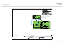
Pin Signal
P3.1 Input 1
P3.2 Input 2
P3.3 Input 3
P3.4 Input 4
P3.5 Input 5
P3.6 Input 6
P3.7 Input 7
P3.8 GND for inputs 1-7
P3.9 unused
P3.10 Output 5, NC
P3.11 Output 5, NO
P3.12 Output 5, COM
P4.1 Output 6, NC
P4.2 Output 6, NO
P4.3 Output 6, COM
P4.4 Output 7, NC
P4.5 Output 7, NO
P4.6 Output 7, COM
P4.7 Output 8, NC
P4.8 Output 8, NO
P4.9 Output 8, COM
P4.10 Output 9, NC
P4.11 Output 9, NO
P4.12 Output 9, COM
P2.1 Output 10, NC
P2.2 Output 10, NO
P2.3 Output 10, COM
P2.4 Output 11, NC
P2.5 Output 11, NO
P2.6 Output 11, COM
P2.7 Output 12, NC
P2.8 Output 12, NO
P2.9 Output 12, COM
P2.10 Output 13, NC
P2.11 Output 13, NO
P2.12 Output 13, COM
Digital inputs
Digital outputs
Terminal
MOD 485/
2 wire
MOD 485/
4 wire
RS 232
P4.4 SER1 Common Common Common
P4.5 SER2
not used not used
RXD
P4.6 SER3
not used not used
TXD
P4.7 SER4
not used
RXD1(+)
not used
P4.8 SER5 D1(+) TXD1(+) Common
P4.9 SER6
not used not used not used
P4.10 7
not used not used not used
P4.11 8
not used
RXD0(-)
not used
P4.12 9 D0(-) TXD0(-)
not used
Assignment of serial interface terminals
X
*) Alternatively on the curcuit card XASI,
the Jumper P2 can be plugged
**) Alternatively on the curcuit card XASI,
the Jumper P1 can be plugged