


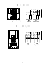

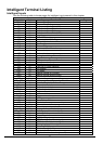
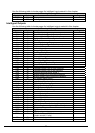
20
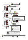
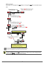
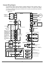
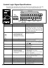
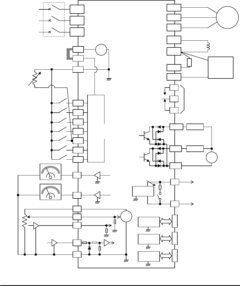
Example Wiring Diagram
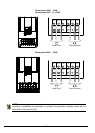
The schematic diagram below provides a general example of logic connector wiring, in
addition to basic power and motor wiring converted in Chapter 2. The goal of this chapter
is to help you determine the proper connections for the various terminals shown below for
your application needs.
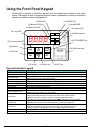
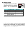
Breaker, MCCB
or GFI
Power source,
3-phase or
1-phase, per
inverter model
AM
Meter
H
L
A
nalog reference
0~10VDC
4~20mA
GND for analog signals
WJ200
Moto
r
PD/+1
P/+
R
(
L1
)
S
(
L2
)
T
N
(
L3
)
U(T1)
V(T2)
W(T3)
N/-
DC reactor
(optional)
AL1
AL0
AL2
Relay contacts,
type 1 Form C
EO
Meter
Pulse train input
24Vdc 32kHz max.
RB
Brake
resistor
(optional)
11/EDM
Load
Freq. arrival signal
Open collector output
Output circuit
GND for logic outputs
12
Load
+
-
CM2
L
+
-
O
OI
EA
A
pprx.10kΩ
10Vdc
A
pprx.100Ω
RS485
transceiver
RJ45 port
(Optional operator port)
USB
transceiver
USB (mini-B) port
(PC communication port)
USB power: Self power
L
L
Option port
controller
Option port connector
L
L
L
L
L
SP
SN
RS485
transceiver
Termination resistor (200
Ω
)
(Change by slide switch)
Serial communication port
(RS485/Modbus)
Forward
Thermistor
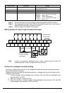
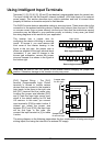
Intelligent inputs,
7 terminals
GND for logic inputs
NOTE: For the wiring
of intelligent I/O and
analog inputs, be sure
to use twisted pair /
shielded cable. Attach
the shielded wire for
each signal to its
respective common
terminal at the inverter
end only.
Input impedance of
each intelligent input is
4.7kΩ
Jumper wire
(Sink logic)
NOTE: Common for
RS485 is “L”.
Braking
unit (optional)
24V
P24
+ -
1
2
3/GS1
4/GS2
5/PTC
6
7/EB
L
PLC
L
Input
circuits
[5] configurable as
discrete input or
thermistor input