


General Information
14
Basic Operation
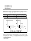
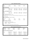
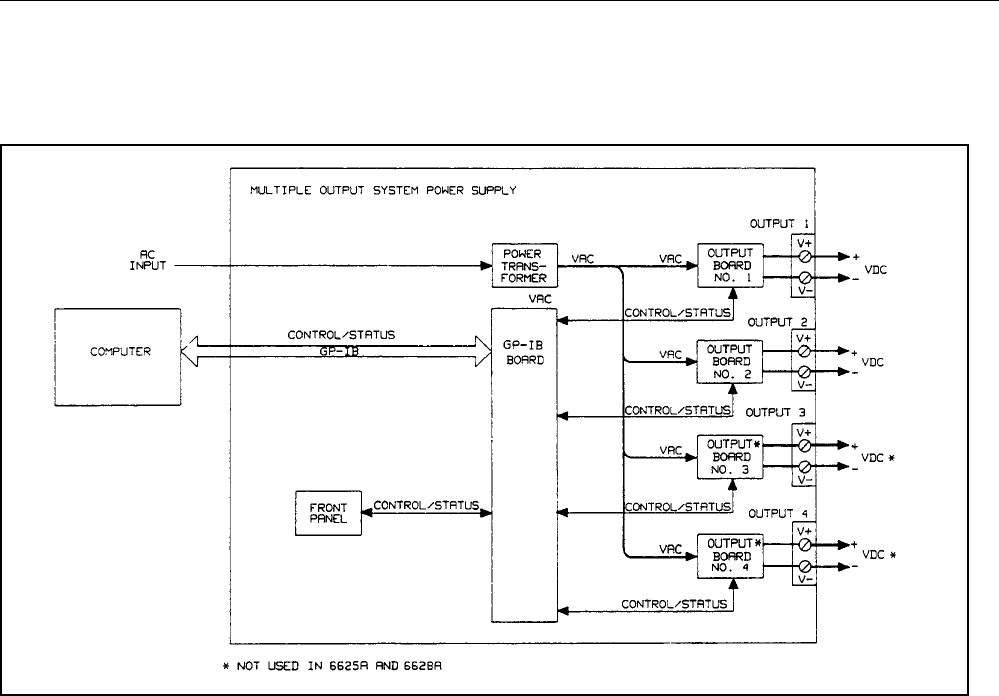
Figure 1-2 is a block diagram that illustrates the major assemblies contained within the power supply. As shown in the
figure, each supply includes a power transformer, two or more output boards, a GP-IB board, and front panel (display and
control keys).
Figure 1-2. Block Diagram
The appropriate ac input voltage is applied to each output board where it is converted to a raw dc voltage which is
subsequently linearly regulated to become the dc output voltage. The magnitude of the output and the mode of operation are
determined by the load and the data received from the GP-IB computer or from the front panel.
Each power supply model contains one output board for each output that it provides.
GP-IB Board
The GP-IB board provides the interface between the user and the multiple outputs of the power supply. Each output board
is actually an output channel that can be individually selected and controlled over the GP-IB or from the supply’s front
panel. Circuits on the GP-IB board interpret commands from the GP-IB or from the front panel to control the selected
output.
The GP-IB board also processes measurement and status data received from the output boards. This data may be read back
over the GP-IB and/or displayed on the supply’s front panel.
The power supply has no potentiometers. Each output is individually calibrated over the GP-IB using calibration commands
(see Appendix A). Correction factors are calculated by the power supply during calibration and are stored in a non-volatile
memory which is located on the supply’s GP-IB board. The supply contains no batteries.