Chapter 2 Function Reference — ICTR_Setup
NI-DAQ FRM for PC Compatibles 2-252
©
National Instruments Corporation
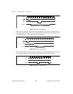
Figure 2-32.
Mode 0 Timing Diagram
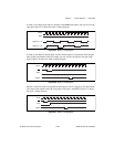
In mode 1, the output goes low on the count following the rising edge of the gate input and
goes high on terminal count. The value of the counter before the rising edge of the gate input
is undefined, Figure 2-33 shows the mode 1 timing diagram.
Figure 2-33.
Mode 1 Timing Diagram
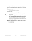
In mode 2, the output goes low for one period of the clock input. count indicates the period
from one output pulse to the next. Figure 2-34 shows the mode 2 timing diagram.
Figure 2-34.
Mode 2 Timing Diagram
Clock
WR
Gate
O
utput
654 3 210
(n = 6)
ABA + B = n
Clock
Gate
Output
n = 4
43210
WR
Clock
Output
Gate
423 1 0 (4)
32 1
n = 4
0 (4)


